Opracowanie technologii cienkich warstw ZnO i...
25
Opracowanie technologii cienkich warstw ZnO i optymalizacja parametrów elektrycznych do złącz Schottky’ego ZnO/metal ElŜbieta Guziewicz, Marek Godlewski T. Krajewski, Ł. Wachnicki, G. Łuka, K. Kopalko, M. Łukasiewicz, E. Łusakowska, E. Przeździecka, I. Kowalik, W. Paszkowicz, P. Kruszewski, P. DłuŜewski Institute of Physics Polish Academy of Sciences NANOBIOM 3 luty 2009
Transcript of Opracowanie technologii cienkich warstw ZnO i...
Opracowanie technologii cienkich
warstw ZnO i optymalizacja
parametrów elektrycznych do złącz
Schottky’ego ZnO/metal
ElŜbieta Guziewicz, Marek GodlewskiT. Krajewski, Ł. Wachnicki, G. Łuka, K. Kopalko,
M. Łukasiewicz, E. Łusakowska, E. Przeździecka, I. Kowalik, W. Paszkowicz, P. Kruszewski, P. DłuŜewski
Institute of PhysicsPolish Academy of Sciences
NANOBIOM 3 luty 2009
Outline
� Atomic Layer Deposition
� ALD laboratory at IF PAN
� ZnO by ALD (precursors, growth rate, structural properties)
� Electrical properties of ZnO-ALD
� Summary
NANOBIOM 3 luty 2009
Atomic Layer Deposition
NANOBIOM 3 luty 2009
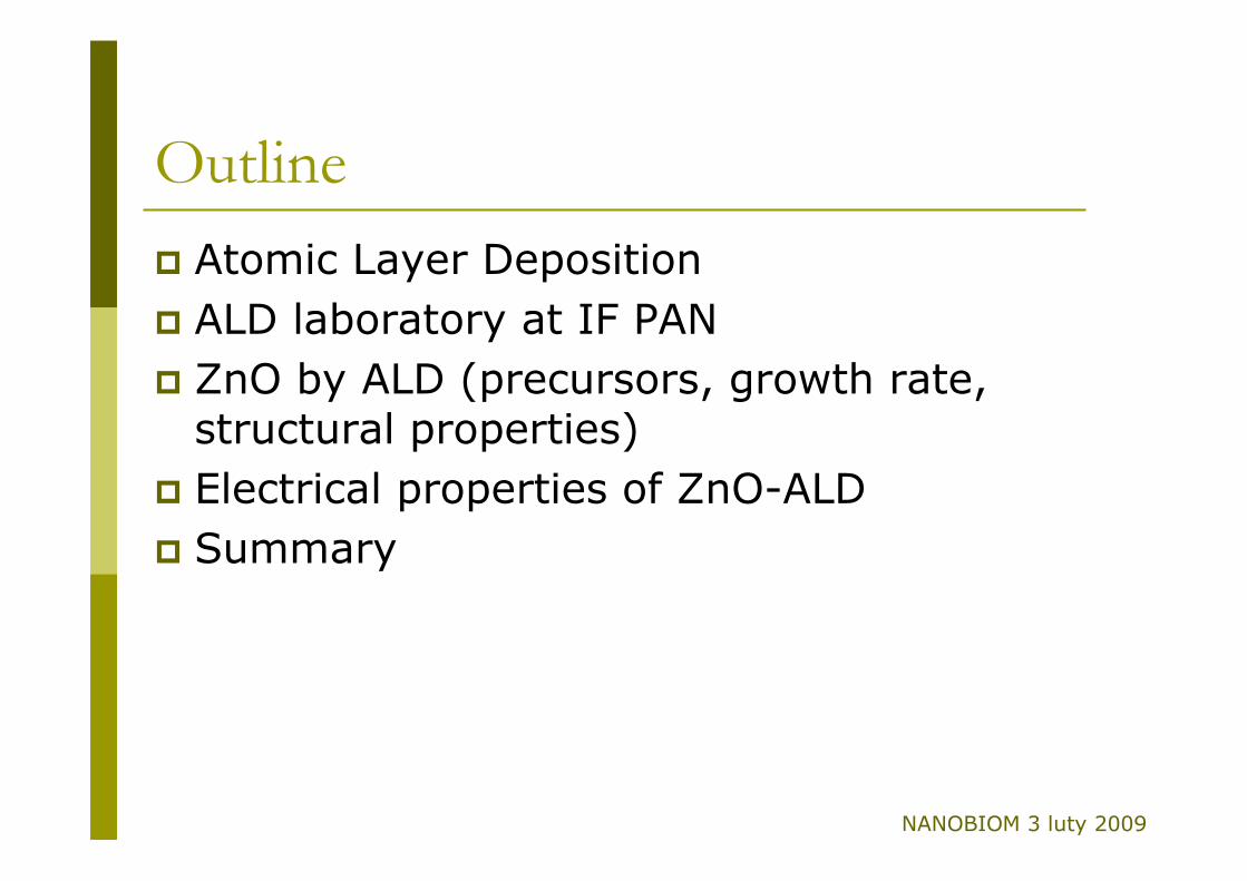
� ALD guarantees flat, uniform and reproducible thickness, low stress, uniform stoichiometry and low defect density.
� Besides the industrial silicon platforms, ALD has proven essential to create gate dielectrics on device substrates without native oxides, such as high mobilityGaAs/AlGaAs heterostructures, organic transistors, nanotubes and many more. Examples of materials include HfO2, ZrO2, Al2O3, LaAlO, GdScO3, their nanolaminates, and others.
Intel has recently announced that their 45 nm generation processors will include a high-k HfO 2 gate dielectric made by ALD .
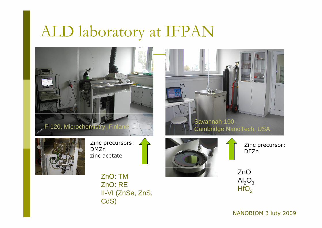
ALD laboratory at IFPAN
NANOBIOM 3 luty 2009
F-120, Microchemistry, FinlandSavannah-100Cambridge NanoTech, USA
ZnO: TMZnO: REII-VI (ZnSe, ZnS,CdS)
ZnOAl2O3HfO2
Zinc precursors:DMZnzinc acetate
Zinc precursor:DEZn
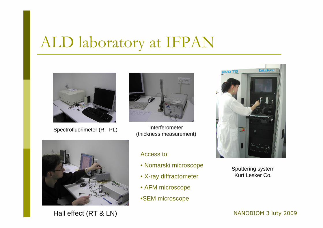
ALD laboratory at IFPAN
NANOBIOM 3 luty 2009
Sputtering system Kurt Lesker Co.
Hall effect (RT & LN)
Interferometer(thickness measurement)
Spectrofluorimeter (RT PL)
Access to:
• Nomarski microscope
• X-ray diffractometer
• AFM microscope
•SEM microscope
ZnO grown by ALD
NANOBIOM 3 luty 2009
� Atomic Layer Deposition
� ALD laboratory at IF PAN
� ZnO by ALD (precursors, growth rate, structural properties)
� Electrical properties of ZnO-ALD
� Summary
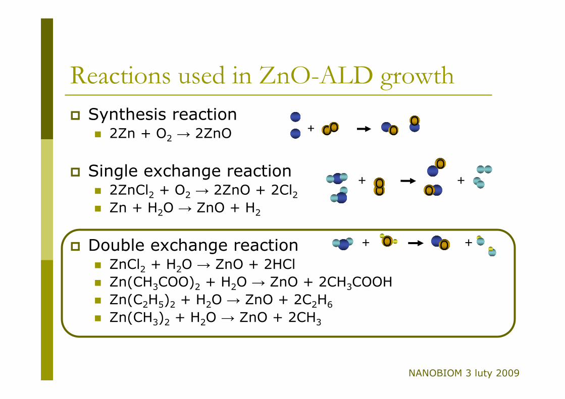
Reactions used in ZnO-ALD growth
NANOBIOM 3 luty 2009
� Synthesis reaction� 2Zn + O2 → 2ZnO
� Single exchange reaction� 2ZnCl2 + O2 → 2ZnO + 2Cl2� Zn + H2O → ZnO + H2
� Double exchange reaction� ZnCl2 + H2O → ZnO + 2HCl
� Zn(CH3COO)2 + H2O → ZnO + 2CH3COOH
� Zn(C2H5)2 + H2O → ZnO + 2C2H6
� Zn(CH3)2 + H2O → ZnO + 2CH3
OO
O
O
O O
OO OO
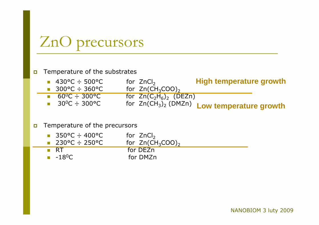
ZnO precursors
NANOBIOM 3 luty 2009
� Temperature of the substrates
� 430°C ÷ 500°C for ZnCl2� 300°C ÷ 360°C for Zn(CH3COO)2
� 600C ÷ 300°C for Zn(C2H6)2 (DEZn)� 300C ÷ 300°C for Zn(CH3)2 (DMZn)
� Temperature of the precursors
� 350°C ÷ 400°C for ZnCl2� 230°C ÷ 250°C for Zn(CH3COO)2
� RT for DEZn� -180C for DMZn
High temperature growth
Low temperature growth
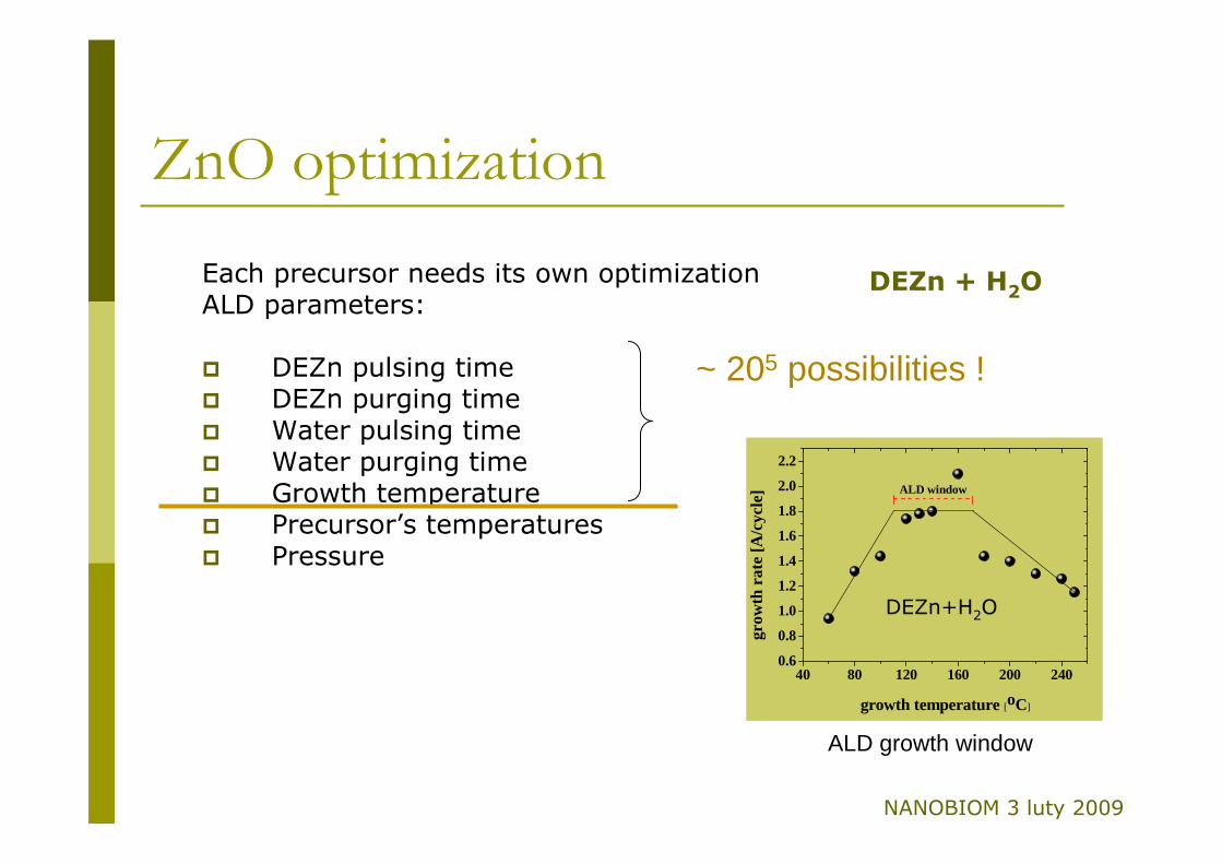
ZnO optimization
NANOBIOM 3 luty 2009
Each precursor needs its own optimizationALD parameters:
� DEZn pulsing time� DEZn purging time� Water pulsing time� Water purging time� Growth temperature� Precursor’s temperatures� Pressure
~ 205 possibilities !
40 80 120 160 200 2400.6
0.8
1.0
1.2
1.4
1.6
1.8
2.0
2.2
grow
th r
ate
[A/c
ycle
]
growth temperature [oC]
ALD window
ALD growth window
DEZn+H2O
DEZn + H2O
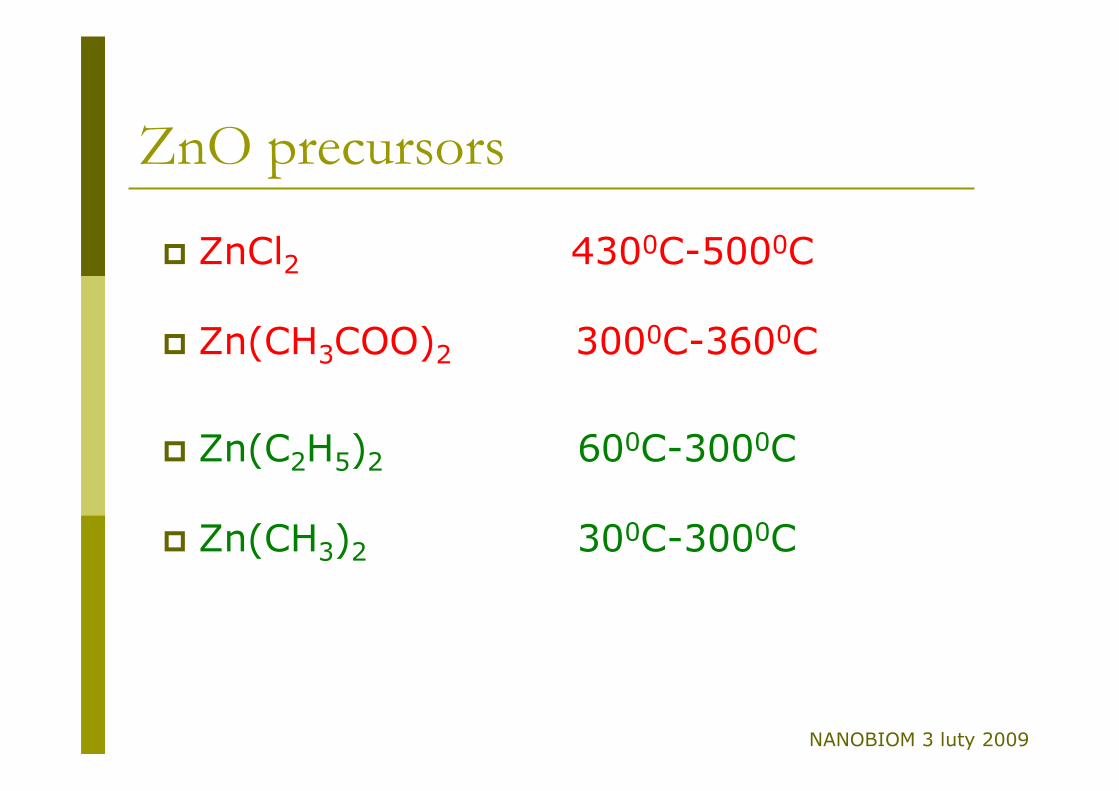
ZnO precursors
� ZnCl2 4300C-5000C
� Zn(CH3COO)2 3000C-3600C
� Zn(C2H5)2 600C-3000C
� Zn(CH3)2 300C-3000C
NANOBIOM 3 luty 2009
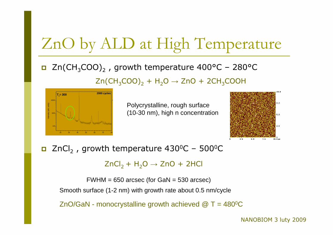
ZnO by ALD at High Temperature
NANOBIOM 3 luty 2009
� Zn(CH3COO)2 , growth temperature 400°C – 280°C
� ZnCl2 , growth temperature 4300C – 5000C
20 30 40 50 60 70 80
100
1000
10000 10000
Inte
nsity
(ar
b. u
nits
)
TS= 300 2000 cycles
Polycrystalline, rough surface (10-30 nm), high n concentration
ZnO/GaN - monocrystalline growth achieved @ T = 4800C
FWHM = 650 arcsec (for GaN = 530 arcsec)
Smooth surface (1-2 nm) with growth rate about 0.5 nm/cycle
ZnCl2 + H2O → ZnO + 2HCl
Zn(CH3COO)2 + H2O → ZnO + 2CH3COOH
Low Temperature ZnO by ALD
NANOBIOM 3 luty 2009
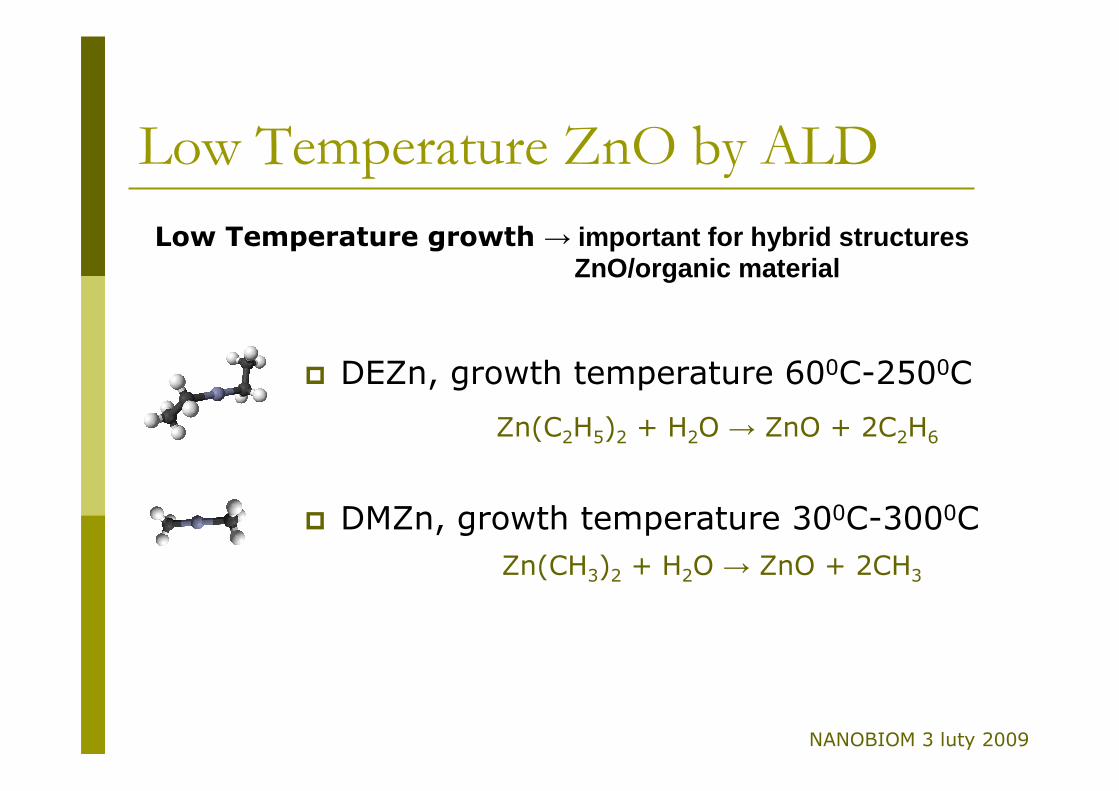
� DEZn, growth temperature 600C-2500C
Zn(C2H5)2 + H2O → ZnO + 2C2H6
� DMZn, growth temperature 300C-3000C
Zn(CH3)2 + H2O → ZnO + 2CH3
Low Temperature growth → important for hybrid structures ZnO/organic material
Low Temperature ZnO by ALD
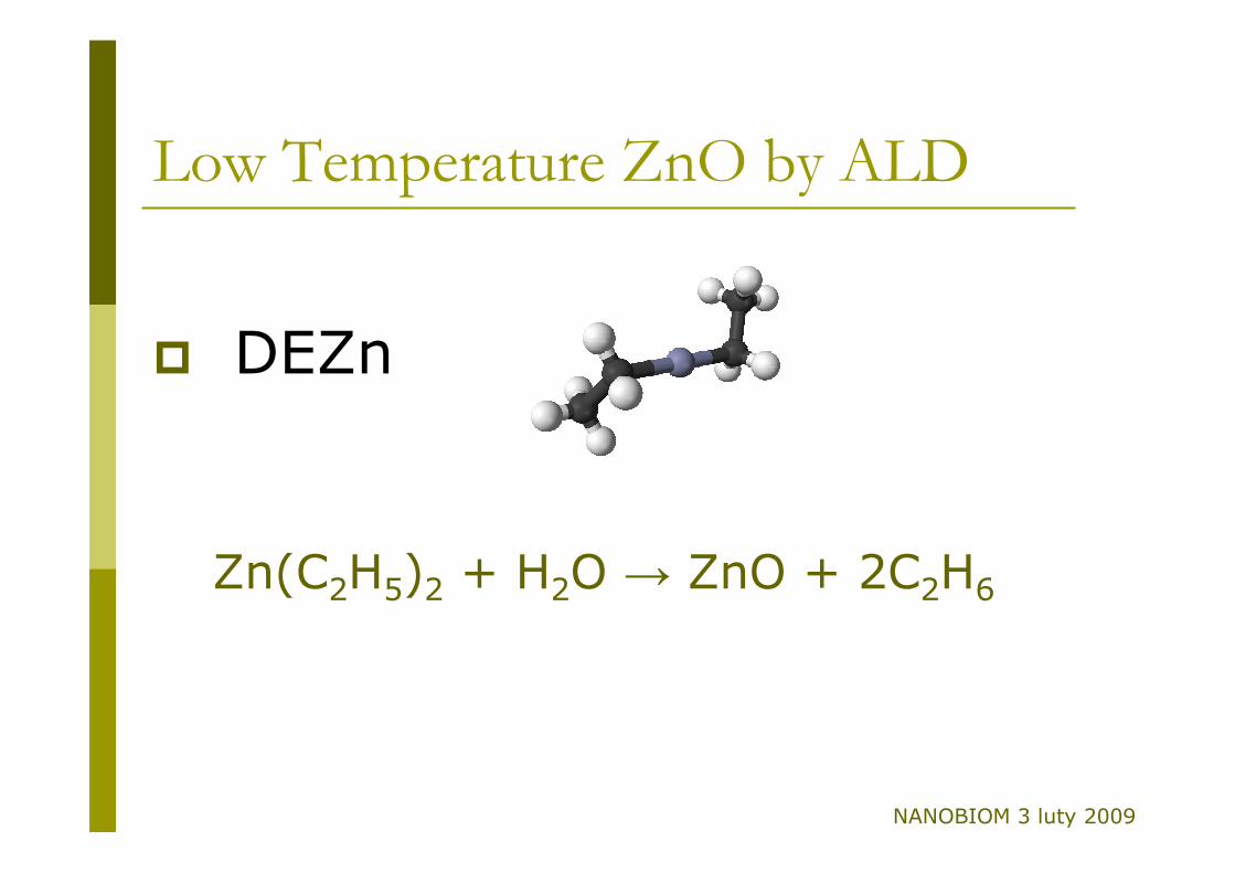
� DEZn
Zn(C2H5)2 + H2O → ZnO + 2C2H6
NANOBIOM 3 luty 2009
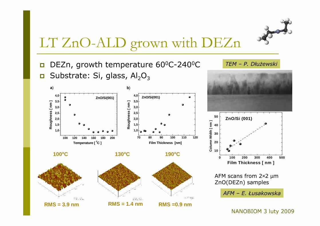
LT ZnO-ALD grown with DEZn
� DEZn, growth temperature 600C-2400C
� Substrate: Si, glass, Al2O3
NANOBIOM 3 luty 2009
b)
100 120 140 160 180 200
1,0
1,5
2,0
2,5
3,0
3,5
4,0
Rou
ghne
ss [
nm ]
Temperature [ 0C ]
ZnO/Si(001)
70 80 90 100 110 120
1,0
1,5
2,0
2,5
3,0
3,5
4,0
Rou
ghne
ss [
nm ]
Film Thickness [nm]
ZnO/Si(001)
a)
100°°°°C 130°°°°C 190°°°°C
RMS = 3.9 nm RMS =0.9 nmRMS = 1.4 nm
AFM scans from 2×2 µm ZnO(DEZn) samples
0 100 200 300 400 500
10
20
30
40
50
Col
umn
Wid
th [
nm ]
Film Thickness [ nm ]
ZnO/Si (001)
AFM – E. Łusakowska
TEM – P. DłuŜewski
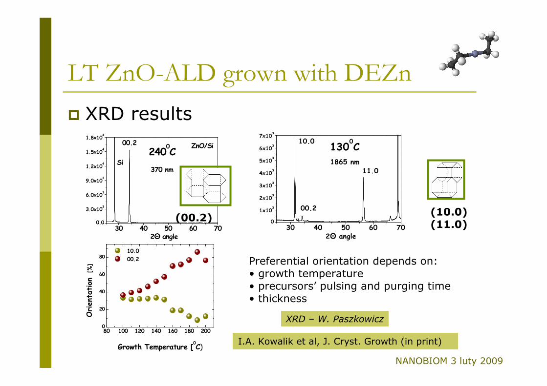
LT ZnO-ALD grown with DEZn
� XRD results
NANOBIOM 3 luty 2009
(10.0)(11.0) 30 40 50 60 70
0.0
3.0x10³
6.0x10³
9.0x10³
1.2x10⁴
1.5x10⁴
1.8x10⁴
ZnO/Si
370 nmSi
2400C
00.2
2ΘΘΘΘ angle30 40 50 60 70
0
1x10³
2x10³
3x10³
4x10³
5x10³
6x10³
7x10³
1865 nm
1300C
10.0
00.2
11.0
2ΘΘΘΘ angle
(00.2)
80 100 120 140 160 180 2000
20
40
60
80 10.0
00.2
Growth Temperature [0C)
Orientation [%]
Preferential orientation depends on:• growth temperature• precursors’ pulsing and purging time• thickness
I.A. Kowalik et al, J. Cryst. Growth (in print)
XRD – W. Paszkowicz
LT ZnO-ALD grown with DEZn
NANOBIOM 3 luty 2009
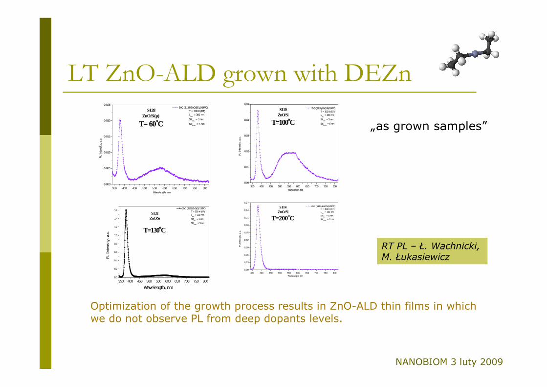
350 400 450 500 550 600 650 700 750 8000.000
0.005
0.010
0.015
0.020
0.025 ZnO (S128/ZnO/Si(p)/60
oC)
T = 300 K (RT)
λexc. = 300 nm
Slitexc. = 5 nm
Slitemm.
= 5 nm
PL Intensity, a.u.
Wanelength, nm
T= 60oC
S128ZnO/Si(p)
350 400 450 500 550 600 650 700 750 8000,00
0,01
0,02
0,03
0,04
0,05 ZnO (S110/ZnO/Si/100
oC)
T = 300 K (RT)
λexc. = 300 nm
Slitexc. = 5 nm
Slitemm.
= 5 nm
PL Intensity, a.u.
Wanelength, nm
T=100oC
S110ZnO/Si
350 400 450 500 550 600 650 700 750 8000,00
0,03
0,06
0,09
0,12
0,15
0,18
0,21
0,24
0,27 ZnO (S114/ZnO/Si/200
oC)
T = 300 K (RT)
λexc.
= 300 nm
Slitexc.
= 5 nm
Slitemm.
= 5 nm
PL Intensity, a.u.
Wanelength, nm
T=200oC
S114ZnO/Si
350 400 450 500 550 600 650 700 750 8000.0
0.2
0.4
0.6
0.8
1.0
1.2
1.4
1.6 ZnO (S132/ZnO/Si/130
oC)
T = 300 K (RT)
λexc. = 300 nm
Slitexc. = 5 nm
Slitemm.
= 5 nm
PL Intensity, a.u.
Wavelength, nm
T=130oC
S132ZnO/Si
Optimization of the growth process results in ZnO-ALD thin films in which we do not observe PL from deep dopants levels.
RT PL – Ł. Wachnicki, M. Łukasiewicz
„as grown samples”
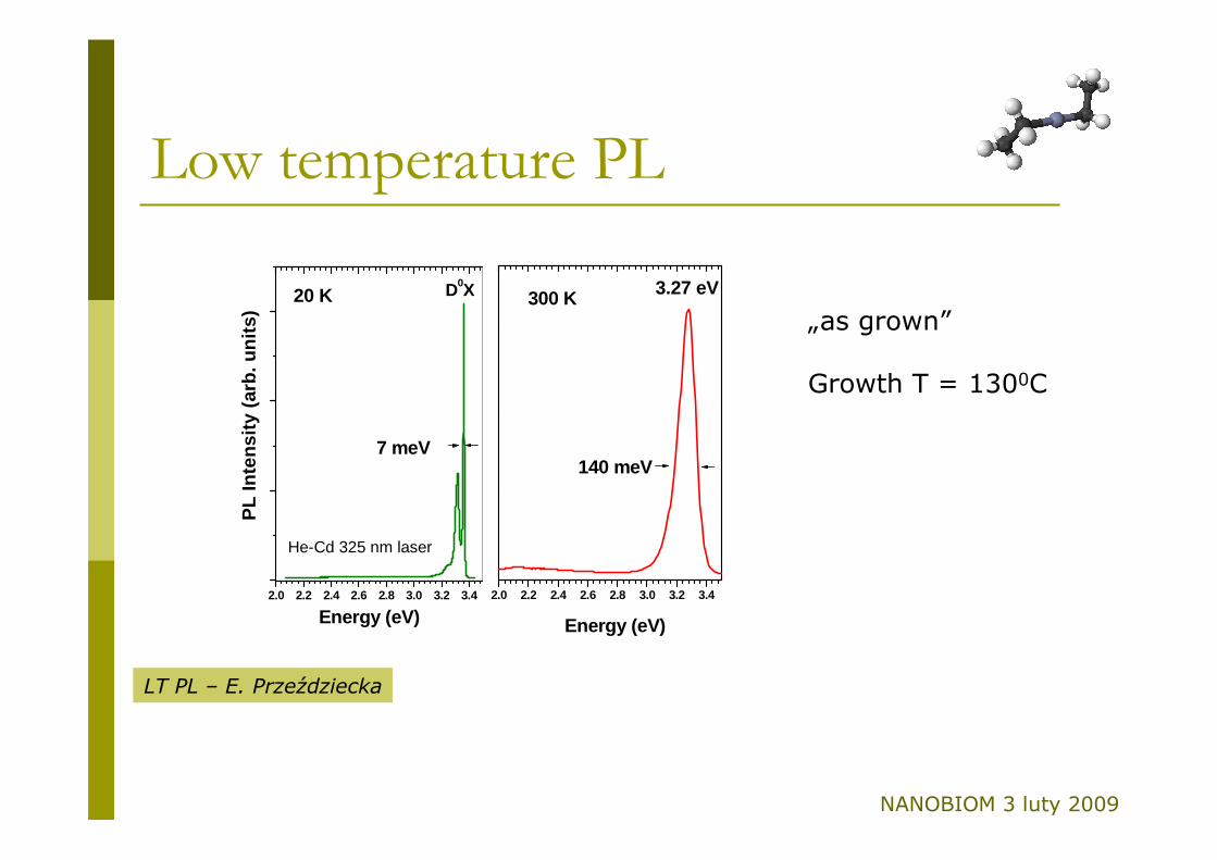
Low temperature PL
NANOBIOM 3 luty 2009
2.0 2.2 2.4 2.6 2.8 3.0 3.2 3.4 2.0 2.2 2.4 2.6 2.8 3.0 3.2 3.4
20 K
Energy (eV)
7 meV
D0X
He-Cd 325 nm laser
P
L In
tens
ity (
arb.
uni
ts)
Energy (eV)
140 meV
3.27 eV300 K
LT PL – E. Przeździecka
„as grown”
Growth T = 1300C
Electrical properties
NANOBIOM 3 luty 2009
For electronic applications a stable and reproducible n- and p-type doping is
obligatory.
nominally undoped ZnO is heavily n-type
Electrical properties
NANOBIOM 3 luty 2009
� nominally undoped ZnO is heavily n-type
� EG(RT) ≅ 3.37 eV → intrinsic free carrier n(RT)~106cm-3
� 1017-1021 cm-3 reported for ZnO grown by different techniques!
� very high level of n-doping has been attributed to different types of defects
� carbonates, hydrogen carbonates, zinc interstitials, oxygen vacancies, hydrogen
often introduce very shallow donor levels at ~ 10÷50 meV below the CV minimum
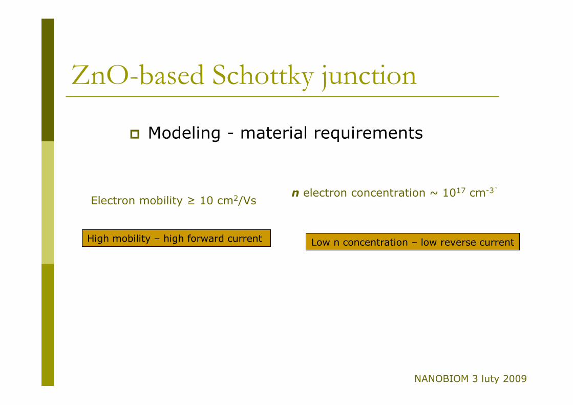
ZnO-based Schottky junction
� Modeling - material requirements
High mobility – high forward current Low n concentration – low reverse current
n electron concentration ~ 1017 cm-3`
Electron mobility ≥ 10 cm2/Vs
NANOBIOM 3 luty 2009
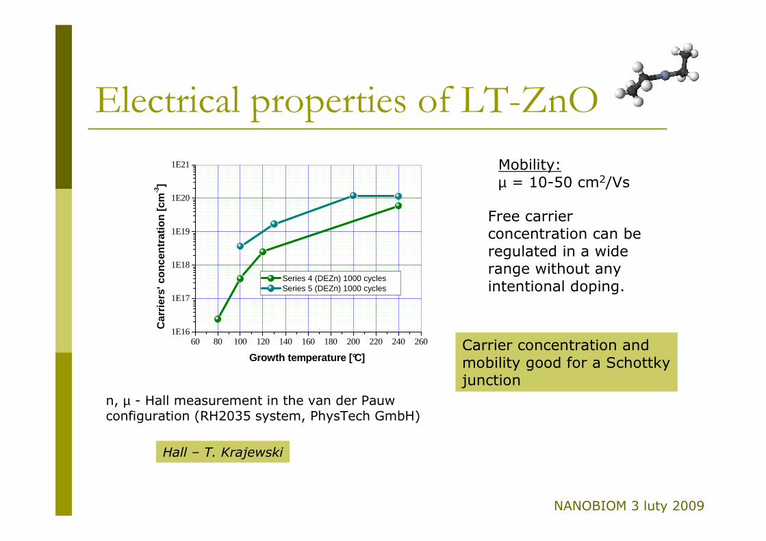
Electrical properties of LT-ZnO
NANOBIOM 3 luty 2009
60 80 100 120 140 160 180 200 220 240 2601E16
1E17
1E18
1E19
1E20
1E21C
arrie
rs' c
once
ntra
tion
[cm
-3]
Growth temperature [°C]
Series 4 (DEZn) 1000 cycles Series 5 (DEZn) 1000 cycles
n, µ - Hall measurement in the van der Pauwconfiguration (RH2035 system, PhysTech GmbH)
Free carrier concentration can be regulated in a wide range without any intentional doping.
Mobility:µ = 10-50 cm2/Vs
Hall – T. Krajewski
Carrier concentration and mobility good for a Schottky junction
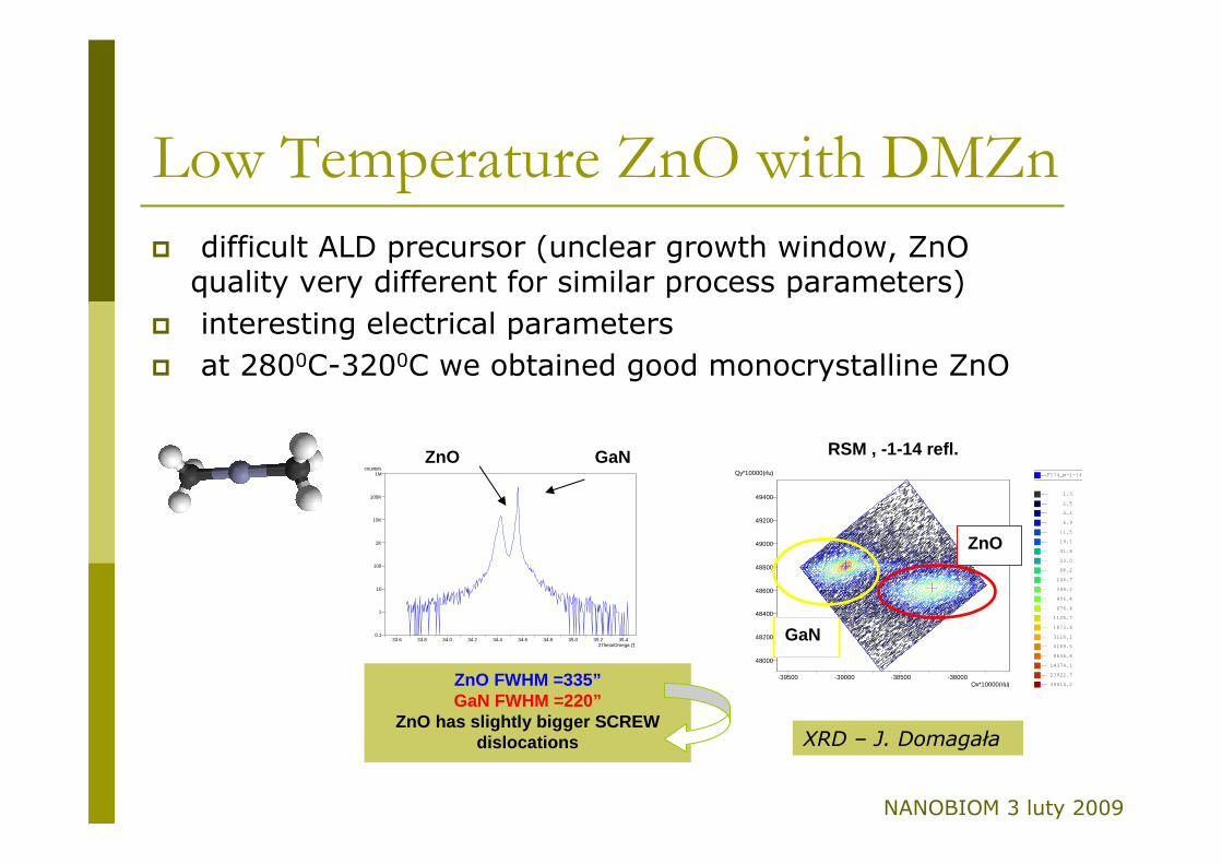
Low Temperature ZnO with DMZn
NANOBIOM 3 luty 2009
� difficult ALD precursor (unclear growth window, ZnO quality very different for similar process parameters)
� interesting electrical parameters
� at 2800C-3200C we obtained good monocrystalline ZnO
-39500 -39000 -38500 -38000Qx*10000(rlu)
48000
48200
48400
48600
48800
49000
49200
49400
Qy*10000(rlu)
S
L
F174_m-1-14_DAslit1i8.xrdml
1.5
2.5
4.1
6.9
11.5
19.1
31.8
53.0
88.2
146.7
244.2
406.4
676.4
1125.7
1873.6
3118.1
5189.5
8636.8
14374.1
23922.7
39814.2
RSM , -1-14 refl.
ZnO
GaN
ZnO FWHM =335”GaN FWHM =220”
ZnO has slightly bigger SCREW dislocations
33.6 33.8 34.0 34.2 34.4 34.6 34.8 35.0 35.2 35.42Theta/Omega (°)
0.1
1
10
100
1K
10K
100K
1Mcounts/s
ZnO GaN
XRD – J. Domagała
Optimization of growth temperature
� Low temperature → lower n concentration, polycrystalline films
� High temperature → monocrystalline films, high n concentration
NANOBIOM 3 luty 2009
Co wiemy
� Jak kontrolować parametry strukturalne i elektryczne ZnO
� Jak otrzymać monokrystaliczne ZnO (pierwsze wyniki)
� Jak zrobić struktury hybrydowe ZnO/ materiał organiczny
� Jak robić kontakty do n-ZnO (do diod Schottky’ego)
NANOBIOM 3 luty 2009
Jak dalej optymalizować wzrost?
� Własności warstw ZnO dopasowane do danego typu funkcjonalizacji
� Optymalizacja kontaktów
� Problem ZnO p-typu
� Struktury ZnO/GaN oraz GaN/ZnO
� Tlenki podbramkowe do struktur HEMT
NANOBIOM 3 luty 2009


![Katedra Fizyki Ciała Stałego Uniwersytetu Łódzkiego ... · Ćwiczenia laboratoryjne z fizyki cienkich warstw Skrypt Politechniki Wrocławskiej, Wrocław 1975, rozdz. 1 i 2. [2]](https://static.fdocuments.pl/doc/165x107/5c7866d709d3f23a068cc00f/katedra-fizyki-ciala-stalego-uniwersytetu-lodzkiego-cwiczenia-laboratoryjne.jpg)