Mikroskopia elektronowa elektronowy mikroskop transmisyjny...
49
Mikroskopia elektronowa elektronowy mikroskop transmisyjny Transmission Electron Microscopy (TEM) • Zasada działania • Historia ‘odkryć’ • Zastosowane rozwiązania • Przykłady zastosowań Bolesław AUGUSTYNIAK
Transcript of Mikroskopia elektronowa elektronowy mikroskop transmisyjny...
Mikroskopia elektronowaelektronowy mikroskop transmisyjnyTransmission Electron Microscopy
(TEM)
• Zasada działania• Historia ‘odkryć’• Zastosowane rozwiązania• Przykłady zastosowań
Bolesław AUGUSTYNIAK
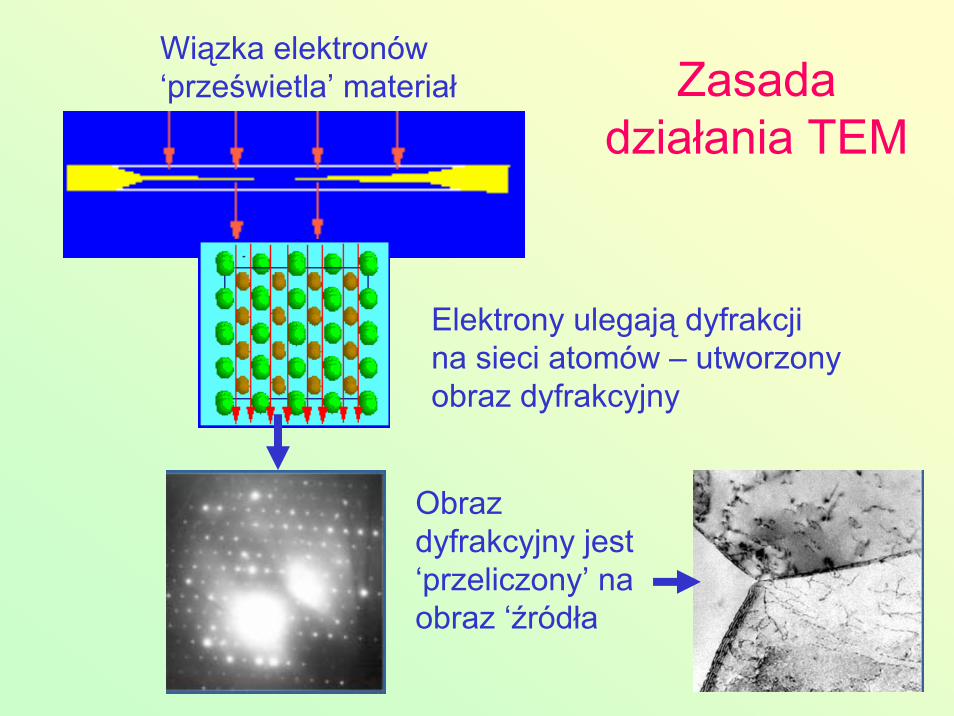
Zasada działania TEM
Wiązka elektronów ‘prześwietla’ materiał
Elektrony ulegają dyfrakcji na sieci atomów – utworzony obraz dyfrakcyjny
Obraz dyfrakcyjny jest ‘przeliczony’ na obraz ‘źródła
Dlaczego TEM ?
mikroskop optyczny
granice ‘fizyczne’ rozdzielczości mikroskopu optycznego
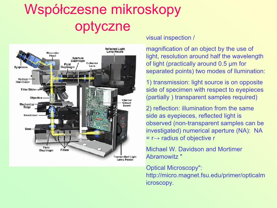
Współczesne mikroskopy optyczne
visual inspection /
magnification of an object by the use of light, resolution around half the wavelength of light (practically around 0.5 µm for separated points) two modes of llumination:
1) transmission: light source is on opposite side of specimen with respect to eyepieces(partially ) transparent samples required)
2) reflection: illumination from the same side as eyepieces, reflected light is observed (non-transparent samples can be investigated) numerical aperture (NA): NA = r→ radius of objective r
Michael W. Davidson and Mortimer Abramowitz "
Optical Microscopy": http://micro.magnet.fsu.edu/primer/opticalmicroscopy.
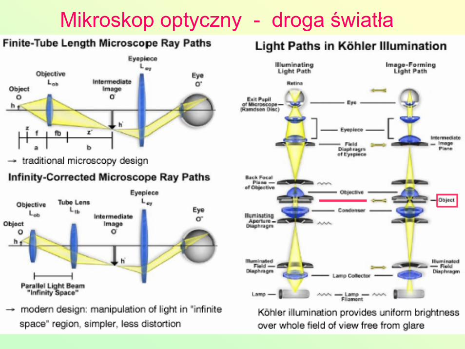
Mikroskop optyczny - droga światła
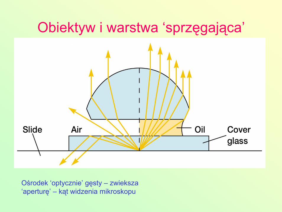
Obiektyw i warstwa ‘sprzęgająca’
Ośrodek ‘optycznie’ gęsty – zwieksza ‘aperturę’ – kąt widzenia mikroskopu
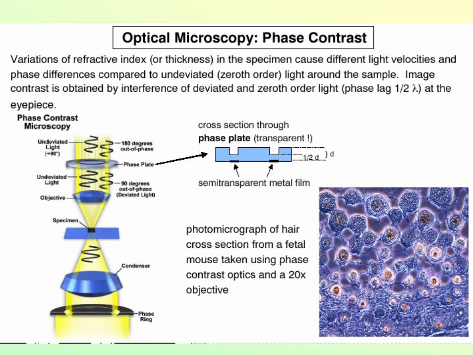
OP - Phase contrast
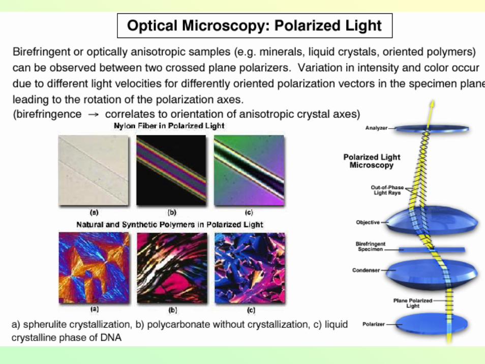
OP – polarized light
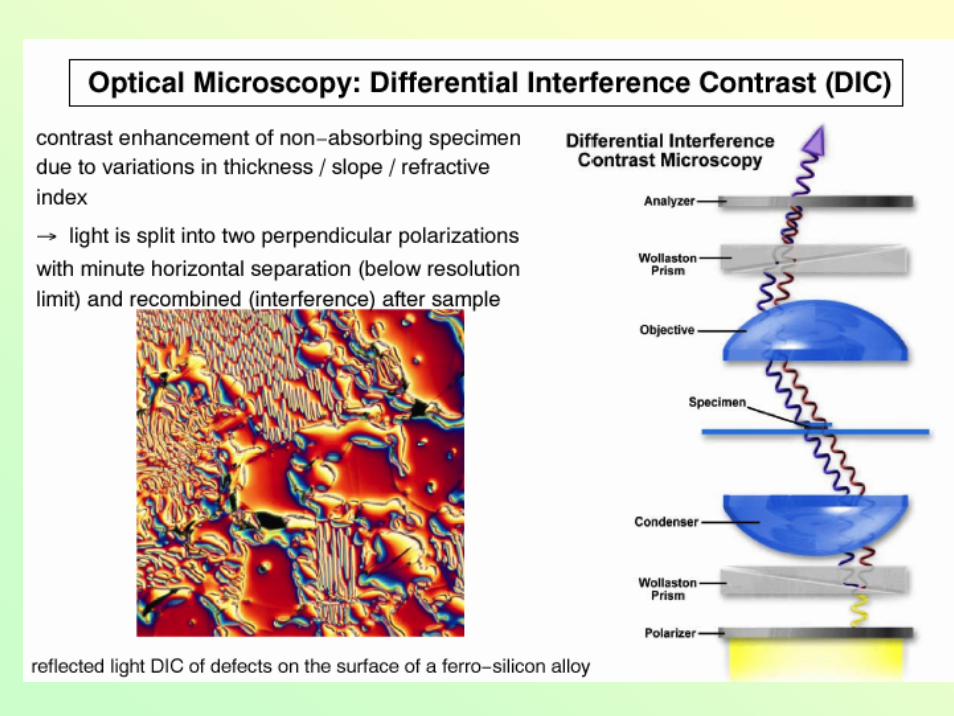
OP – DIC

OP – Fluorescence
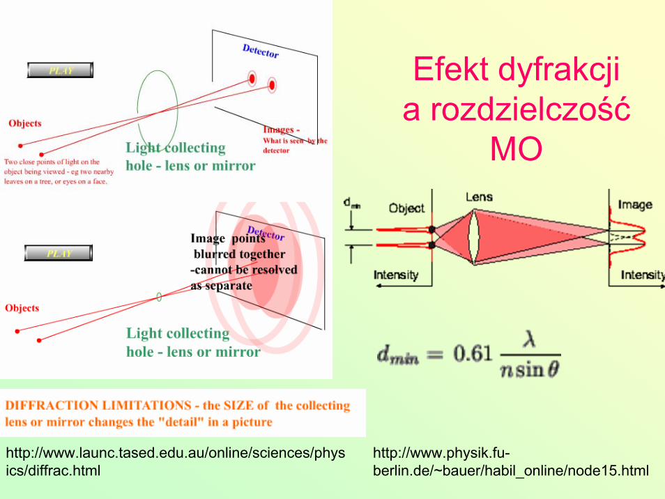
Efekt dyfrakcji a rozdzielczość
MO
http://www.launc.tased.edu.au/online/sciences/physics/diffrac.html
http://www.physik.fu-berlin.de/~bauer/habil_online/node15.html
Efekt dyfrakcji a rozdzielczość MO - cd
http://www.physik.fu-berlin.de/~bauer/habil_online/node15.html
In high-resolving microscopes, oil-immersion objectives with apertures are used, resulting in a maximum resolution of .The Rayleigh criterion is derived under the assumption of incoherent light. For coherent light, under certain circumstances, the resolution can slightly be enhanced to However, (non-scanning) coherent light microscopy is difficult since the images are often superimposed with diffraction patterns that originate from small structures in the optical path. Highest resolution is obtained by scanning confocal microscopy. Here, the image of an illuminating aperture in the sample plane coincides with the "back-focused" image of the exit aperture. Although the size of the illumination and detection spots are diffraction limited, the effective resolution obtained by the combination of the two (as determined by the width of the product of the two respective Airy discs) is enhanced by a factor . For recording images of a specimen, the illumination spot is scanned bytranslating the sample. In addition to high lateral resolution, confocal microscopy also permits imaging of planes at varying depths within the specimen.
Zwiększenie rozdzielczości -konstruktywne wykorzystanie dyfrakcji
Fale materii de Brodlie’a i doświadczenie Devisona-Germera
Koncepcja de Broglie’a
Dyfrakcja elektronów
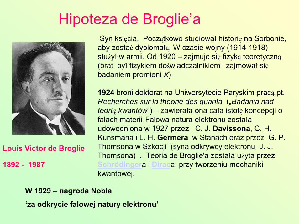
Hipoteza de Broglie’aSyn księcia. Początkowo studiował historię na Sorbonie, aby zostać dyplomatą. W czasie wojny (1914-1918) służył w armii. Od 1920 – zajmuje się fizyką teoretyczną(brat był fizykiem doświadczalnikiem i zajmował siębadaniem promieni X)
1924 broni doktorat na Uniwersytecie Paryskim pracą pt.Recherches sur la théorie des quanta („Badania nad teorią kwantów”) – zawierała ona cała istotę koncepcji o falach materii. Falowa natura elektronu została udowodniona w 1927 przez C. J. Davissona, C. H.Kunsmana i L. H. Germera w Stanach oraz przez G. P.Thomsona w Szkocji (syna odkrywcy elektronu J. J.Thomsona) . Teoria de Broglie'a została użyta przez Schrödingera i Diraca przy tworzeniu mechaniki kwantowej.
W 1929 – nagroda Nobla
‘za odkrycie falowej natury elektronu’
Louis Victor de Broglie
1892 - 1987
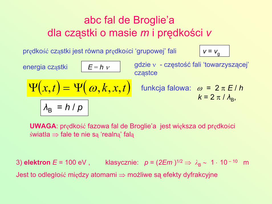
abc fal de Broglie’a dla cząstki o masie m i prędkości v
v = vg
E = h ν
λB = h / p
prędkość cząstki jest równa prędkości ‘grupowej’ fali
energia cząstki gdzie ν - częstość fali ‘towarzyszącej’cząstce
( ) ( )txktx ,,,, ωΨ=Ψ funkcja falowa: ω = 2 π E / h k = 2 π / λB,
UWAGA: prędkość fazowa fal de Broglie’a jest większa od prędkości światła ⇒ fale te nie są ‘realną’ falą
3) elektron E = 100 eV , klasycznie: p = (2Em )1/2 ⇒ λB ∼ 1 ⋅ 10 – 10 m
Jest to odległość między atomami ⇒ możliwe są efekty dyfrakcyjne
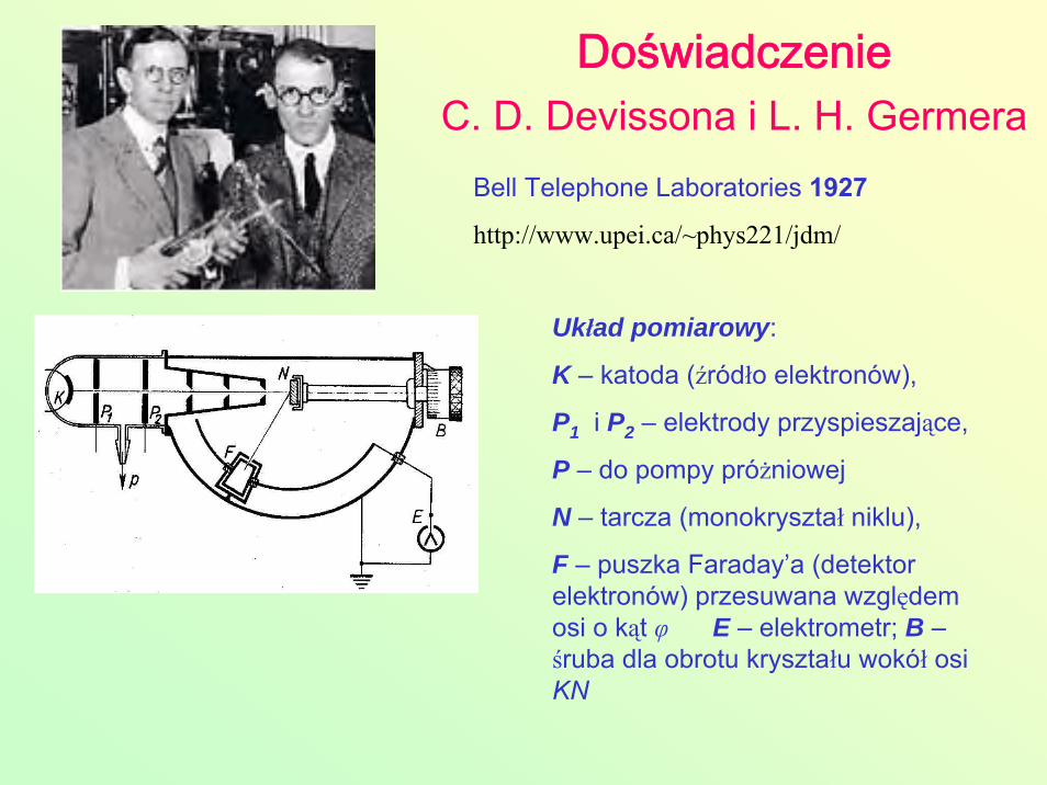
Doświadczenie C. D. Devissona i L. H. Germera
Bell Telephone Laboratories 1927
http://www.upei.ca/~phys221/jdm/
Układ pomiarowy:
K – katoda (źródło elektronów),
P1 i P2 – elektrody przyspieszające,
P – do pompy próżniowej
N – tarcza (monokryształ niklu),
F – puszka Faraday’a (detektor elektronów) przesuwana względem osi o kąt φ E – elektrometr; B –śruba dla obrotu kryształu wokół osi KN
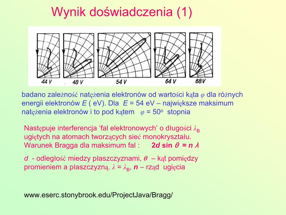
Wynik doświadczenia (1)
badano zależność natężenia elektronów od wartości kąta φ dla różnych energii elektronów E ( eV). Dla E = 54 eV – największe maksimum natężenia elektronów i to pod kątem φ = 50o stopnia
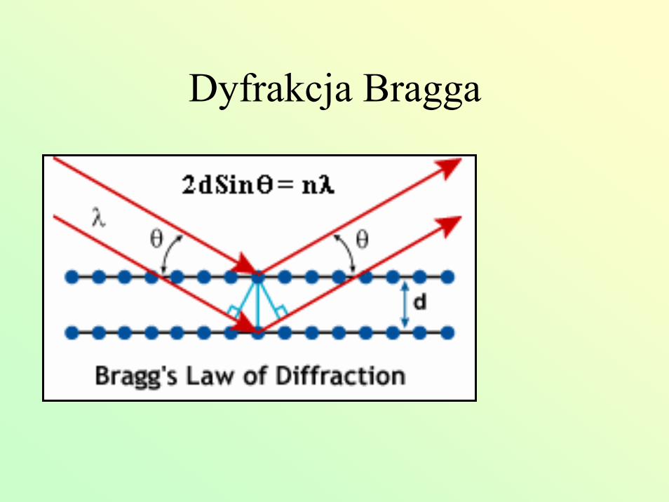
Następuje interferencja ‘fal elektronowych’ o długości λBugiętych na atomach tworzących sieć monokryształu.Warunek Bragga dla maksimum fal : 2d sin θ = n λd - odległość miedzy płaszczyznami, θ – kąt pomiędzy promieniem a płaszczyzną. λ = λB, n – rząd ugięcia
www.eserc.stonybrook.edu/ProjectJava/Bragg/
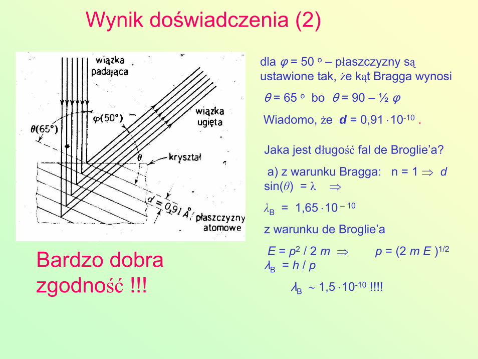
Wynik doświadczenia (2)
dla φ = 50 o – płaszczyzny sąustawione tak, że kąt Bragga wynosi
θ = 65 o bo θ = 90 – ½ φWiadomo, że d = 0,91 ⋅10-10 .
Jaka jest długość fal de Broglie’a?
a) z warunku Bragga: n = 1 ⇒ d sin(θ) = λ ⇒
λB = 1,65 ⋅10 – 10
z warunku de Broglie’a
E = p2 / 2 m ⇒ p = (2 m E )1/2
λB = h / p
λB ∼ 1,5 ⋅10-10 !!!!
Bardzo dobra zgodność !!!
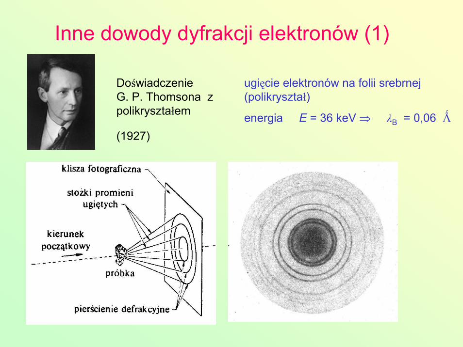
Inne dowody dyfrakcji elektronów (1)
Doświadczenie G. P. Thomsona z polikryształem
(1927)
ugięcie elektronów na folii srebrnej (polikryształ)
energia E = 36 keV ⇒ λB = 0,06 Ǻ
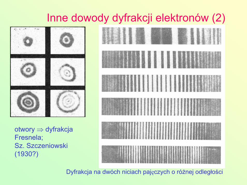
Inne dowody dyfrakcji elektronów (2)
otwory ⇒ dyfrakcja Fresnela; Sz. Szczeniowski(1930?)
Dyfrakcja na dwóch niciach pajęczych o różnej odległości
Dyfrakcja Bragga

abc mikroskopu elektronowegoMikroskopy elektronowe są wykorzystywane gł. w badaniach krystalograf.,biol., med., a także w fizyce. ciała stałego. Pierwszy mikroskop elektronowy zbudowali (wg. Idei mikroskopu optycznego) w 1931. Niemcy M. Knoll i E. Ruska; pierwszy mikroskop elektronowy użytkowy wyprodukowała 1938 firma Siemens.
http://www.republika.pl/technologialaserowa/mikroskop.pdf
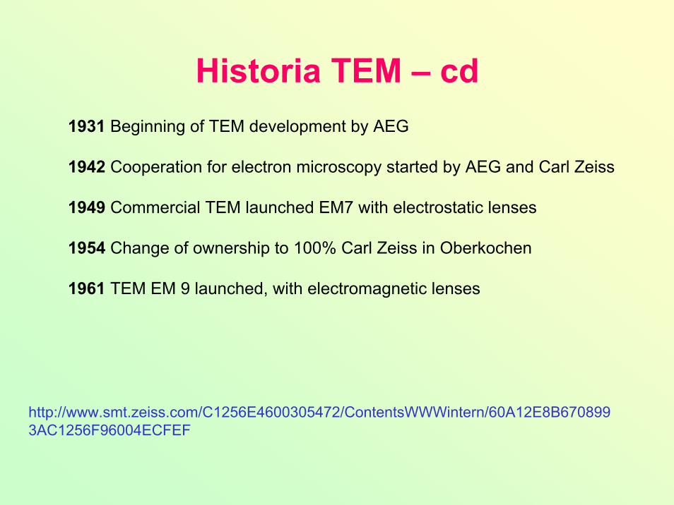
Historia TEM – cd
http://www.smt.zeiss.com/C1256E4600305472/ContentsWWWintern/60A12E8B6708993AC1256F96004ECFEF
1931 Beginning of TEM development by AEG
1942 Cooperation for electron microscopy started by AEG and Carl Zeiss
1949 Commercial TEM launched EM7 with electrostatic lenses
1954 Change of ownership to 100% Carl Zeiss in Oberkochen
1961 TEM EM 9 launched, with electromagnetic lenses
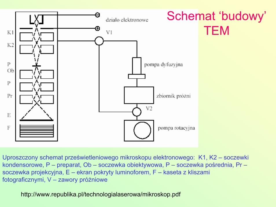
Uproszczony schemat prześwietleniowego mikroskopu elektronowego: K1, K2 – soczewki kondensorowe, P – preparat, Ob – soczewka obiektywowa, P – soczewka pośrednia, Pr –soczewka projekcyjna, E – ekran pokryty luminoforem, F – kaseta z kliszami fotograficznymi, V – zawory próżniowe
Schemat ‘budowy’TEM
http://www.republika.pl/technologialaserowa/mikroskop.pdf
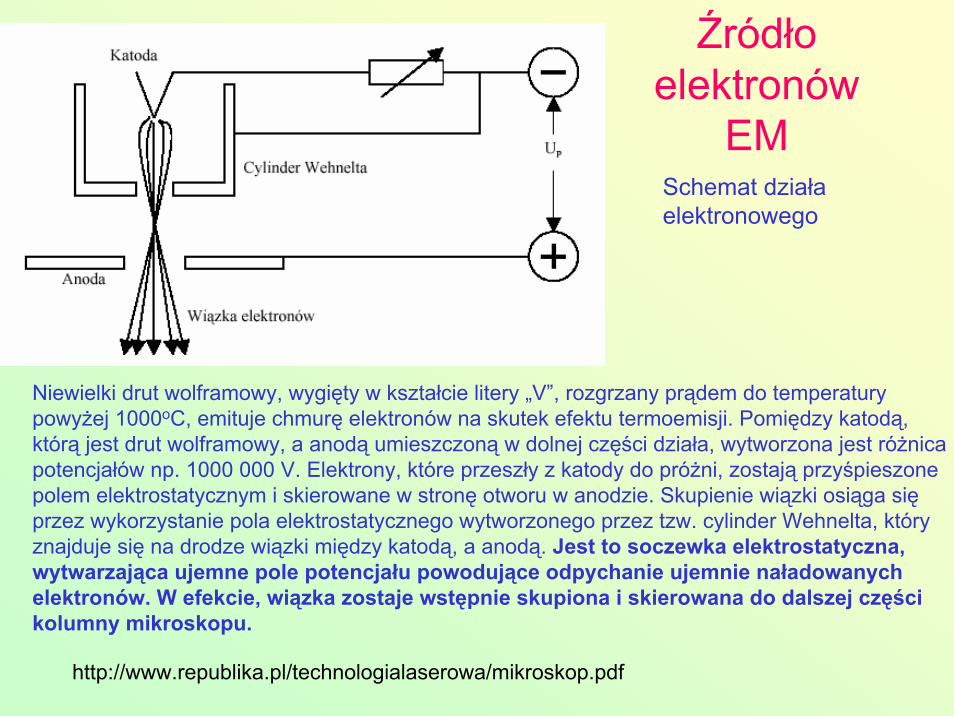
Źródło elektronów
EM
http://www.republika.pl/technologialaserowa/mikroskop.pdf
Schemat działa elektronowego
Niewielki drut wolframowy, wygięty w kształcie litery „V”, rozgrzany prądem do temperatury powyżej 1000oC, emituje chmurę elektronów na skutek efektu termoemisji. Pomiędzy katodą, którą jest drut wolframowy, a anodą umieszczoną w dolnej części działa, wytworzona jest różnica potencjałów np. 1000 000 V. Elektrony, które przeszły z katody do próżni, zostają przyśpieszone polem elektrostatycznym i skierowane w stronę otworu w anodzie. Skupienie wiązki osiąga sięprzez wykorzystanie pola elektrostatycznego wytworzonego przez tzw. cylinder Wehnelta, który znajduje się na drodze wiązki między katodą, a anodą. Jest to soczewka elektrostatyczna, wytwarzająca ujemne pole potencjału powodujące odpychanie ujemnie naładowanych elektronów. W efekcie, wiązka zostaje wstępnie skupiona i skierowana do dalszej części kolumny mikroskopu.
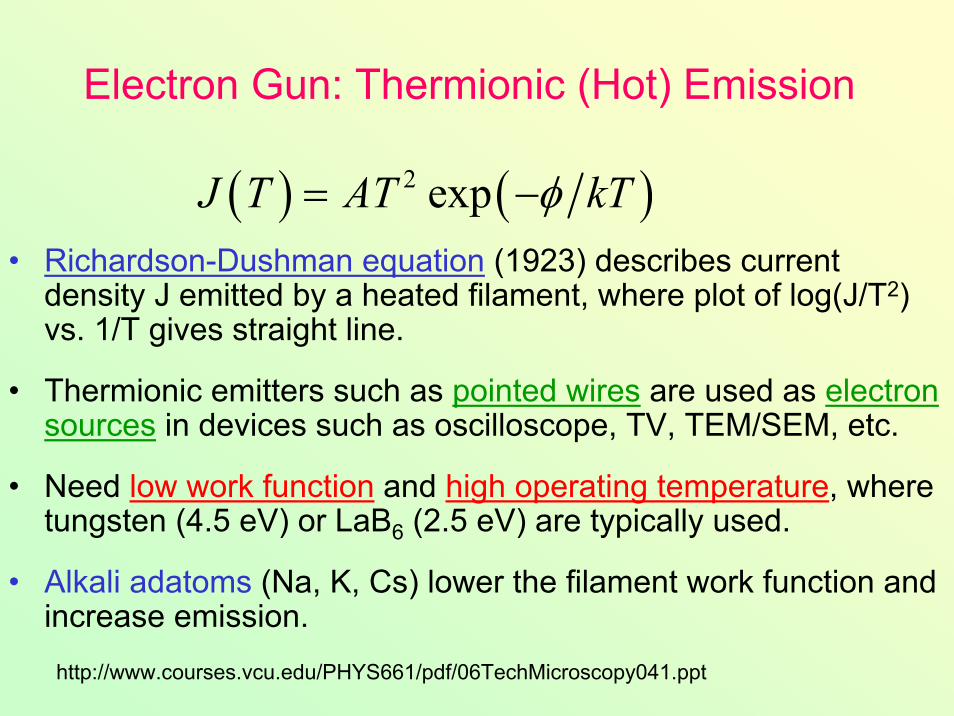
Electron Gun: Thermionic (Hot) Emission
• Richardson-Dushman equation (1923) describes current density J emitted by a heated filament, where plot of log(J/T2) vs. 1/T gives straight line.
• Thermionic emitters such as pointed wires are used as electron sources in devices such as oscilloscope, TV, TEM/SEM, etc.
• Need low work function and high operating temperature, where tungsten (4.5 eV) or LaB6 (2.5 eV) are typically used.
• Alkali adatoms (Na, K, Cs) lower the filament work function and increase emission.
( ) ( )2 expJ T AT kTφ= −
http://www.courses.vcu.edu/PHYS661/pdf/06TechMicroscopy041.ppt
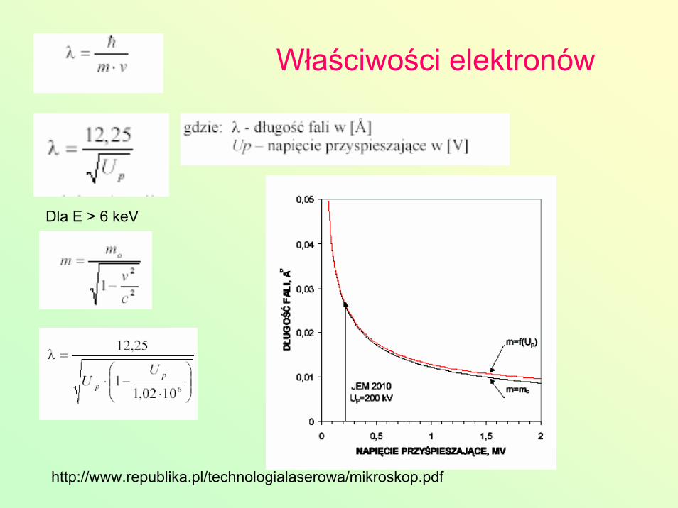
Właściwości elektronów
http://www.republika.pl/technologialaserowa/mikroskop.pdf
Dla E > 6 keV
http://www.republika.pl/technologialaserowa/mikroskop.pdf
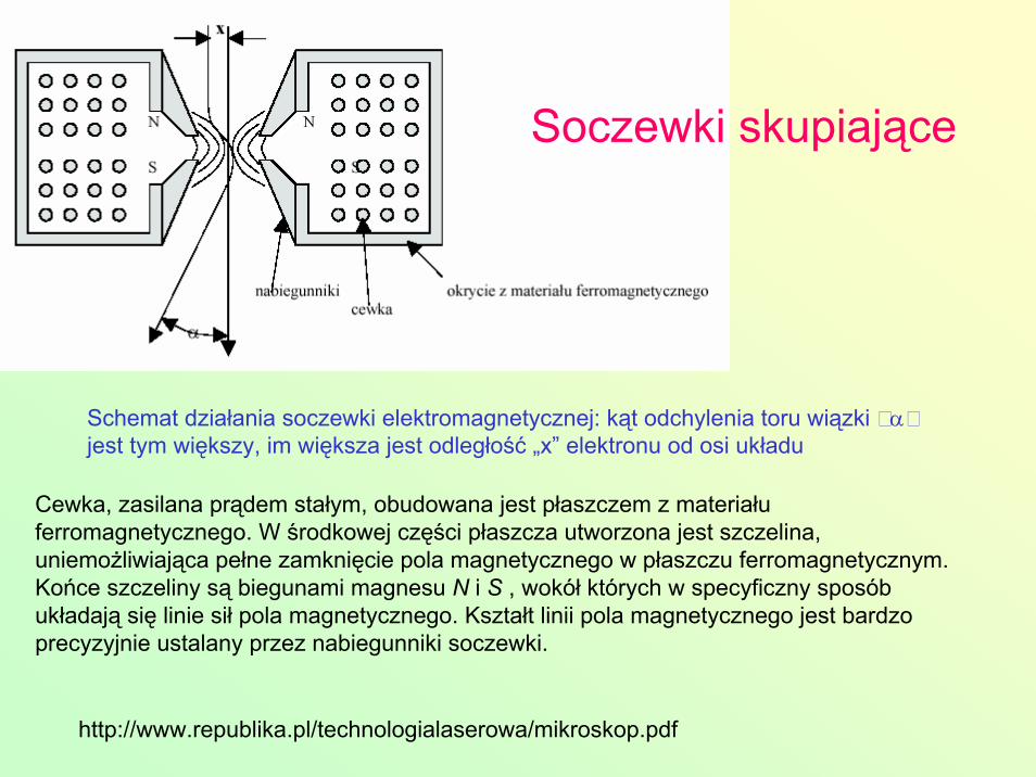
Soczewki skupiające
Cewka, zasilana prądem stałym, obudowana jest płaszczem z materiału ferromagnetycznego. W środkowej części płaszcza utworzona jest szczelina, uniemożliwiająca pełne zamknięcie pola magnetycznego w płaszczu ferromagnetycznym. Końce szczeliny są biegunami magnesu N i S , wokół których w specyficzny sposób układają się linie sił pola magnetycznego. Kształt linii pola magnetycznego jest bardzo precyzyjnie ustalany przez nabiegunniki soczewki.
Schemat działania soczewki elektromagnetycznej: kąt odchylenia toru wiązki αjest tym większy, im większa jest odległość „x” elektronu od osi układu
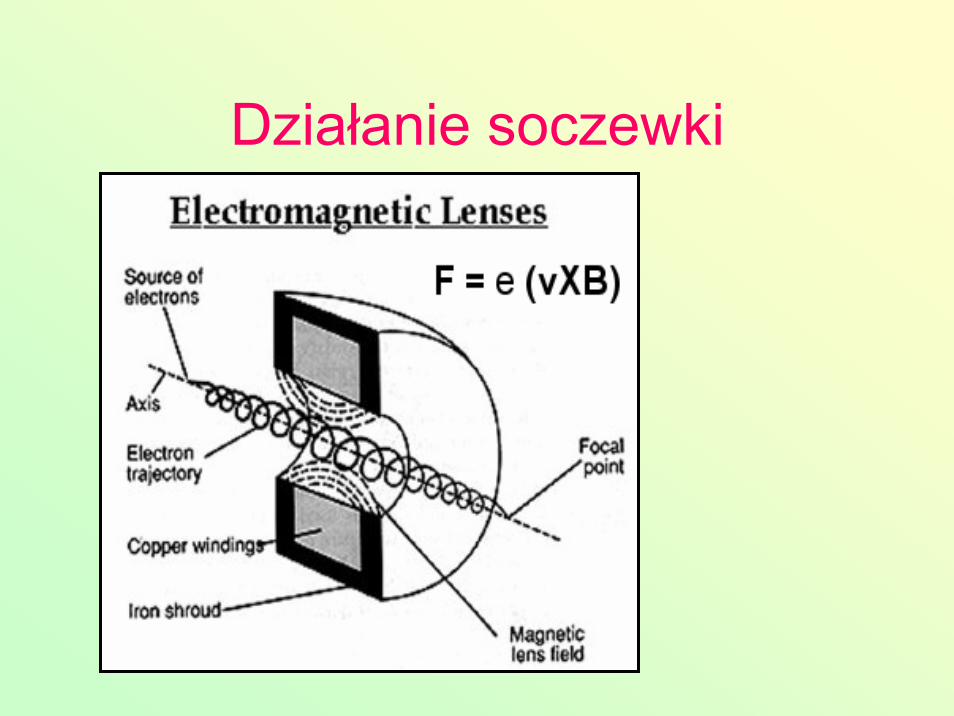
Działanie soczewki
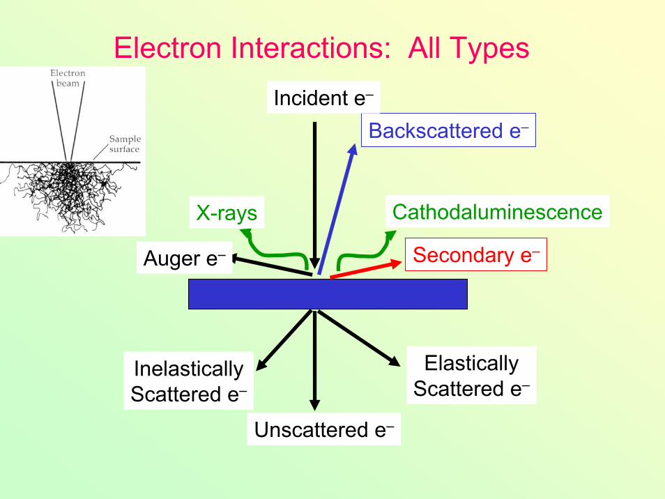
Electron Interactions: All Types
Cathodaluminescence
Secondary e–
Backscattered e–
Incident e–
Auger e–
X-rays
ElasticallyScattered e–
InelasticallyScattered e–
Unscattered e–
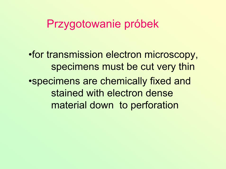
Przygotowanie próbek
•for transmission electron microscopy, specimens must be cut very thin
•specimens are chemically fixed and stained with electron dense material down to perforation
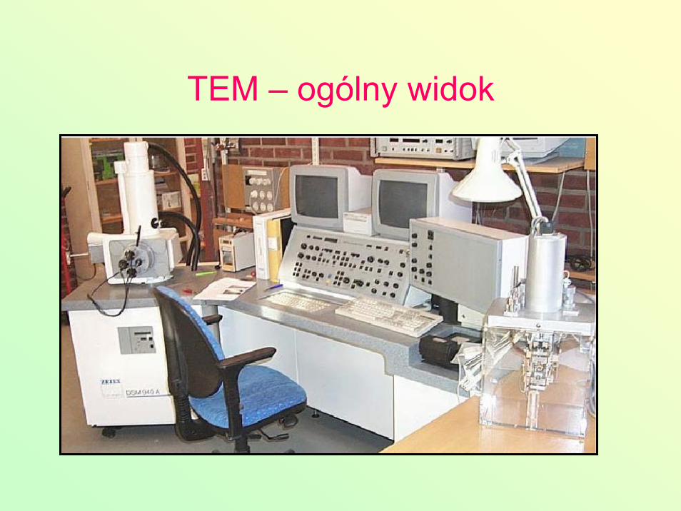
TEM – ogólny widok
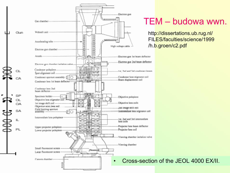
TEM – budowa wwn.
• Cross-section of the JEOL 4000 EX/II.
http://dissertations.ub.rug.nl/FILES/faculties/science/1999/h.b.groen/c2.pdf
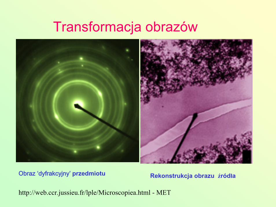
Transformacja obrazów
Rekonstrukcja obrazu źródłaObraz ‘dyfrakcyjny’ przedmiotu
http://web.ccr.jussieu.fr/lple/Microscopiea.html - MET
Obrazy z TEM
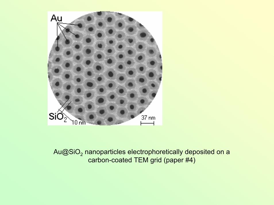
Au@SiO2 nanoparticles electrophoretically deposited on a carbon-coated TEM grid (paper #4)
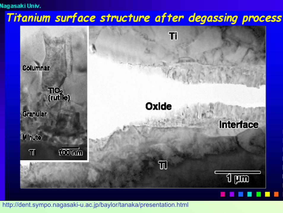
http://dent.sympo.nagasaki-u.ac.jp/baylor/tanaka/presentation.html
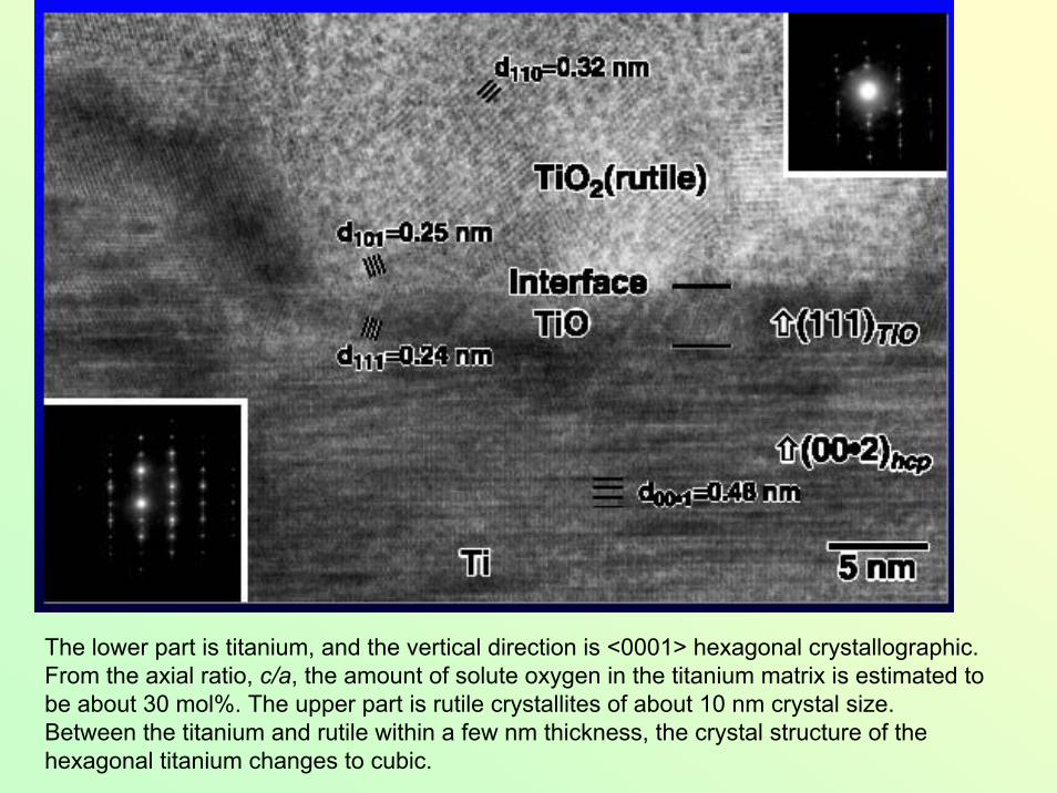
The lower part is titanium, and the vertical direction is <0001> hexagonal crystallographic.From the axial ratio, c/a, the amount of solute oxygen in the titanium matrix is estimated to be about 30 mol%. The upper part is rutile crystallites of about 10 nm crystal size.Between the titanium and rutile within a few nm thickness, the crystal structure of the hexagonal titanium changes to cubic.
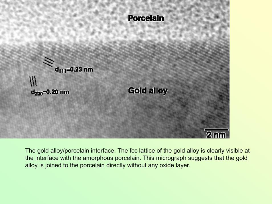
The gold alloy/porcelain interface. The fcc lattice of the gold alloy is clearly visible at the interface with the amorphous porcelain. This micrograph suggests that the gold alloy is joined to the porcelain directly without any oxide layer.
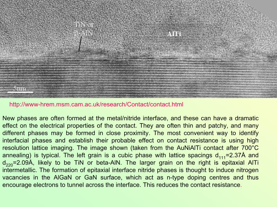
http://www-hrem.msm.cam.ac.uk/research/Contact/contact.html
New phases are often formed at the metal/nitride interface, and these can have a dramatic effect on the electrical properties of the contact. They are often thin and patchy, and many different phases may be formed in close proximity. The most convenient way to identify interfacial phases and establish their probable effect on contact resistance is using high resolution lattice imaging. The image shown (taken from the AuNiAlTi contact after 700°Cannealing) is typical. The left grain is a cubic phase with lattice spacings d111=2.37Å andd220=2.09Å, likely to be TiN or beta-AlN. The larger grain on the right is epitaxial AlTi intermetallic. The formation of epitaxial interface nitride phases is thought to induce nitrogen vacancies in the AlGaN or GaN surface, which act as n-type doping centres and thus encourage electrons to tunnel across the interface. This reduces the contact resistance.
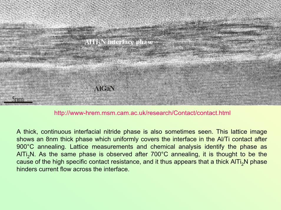
http://www-hrem.msm.cam.ac.uk/research/Contact/contact.html
A thick, continuous interfacial nitride phase is also sometimes seen. This lattice image shows an 8nm thick phase which uniformly covers the interface in the Al/Ti contact after900°C annealing. Lattice measurements and chemical analysis identify the phase as AlTi2N. As the same phase is observed after 700°C annealing, it is thought to be the cause of the high specific contact resistance, and it thus appears that a thick AlTi2N phasehinders current flow across the interface.
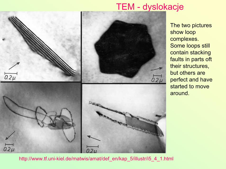
TEM - dyslokacje
The two pictures show loop complexes.Some loops still contain stacking faults in parts oft their structures, but others are perfect and have started to move around.
http://www.tf.uni-kiel.de/matwis/amat/def_en/kap_5/illustr/i5_4_1.html
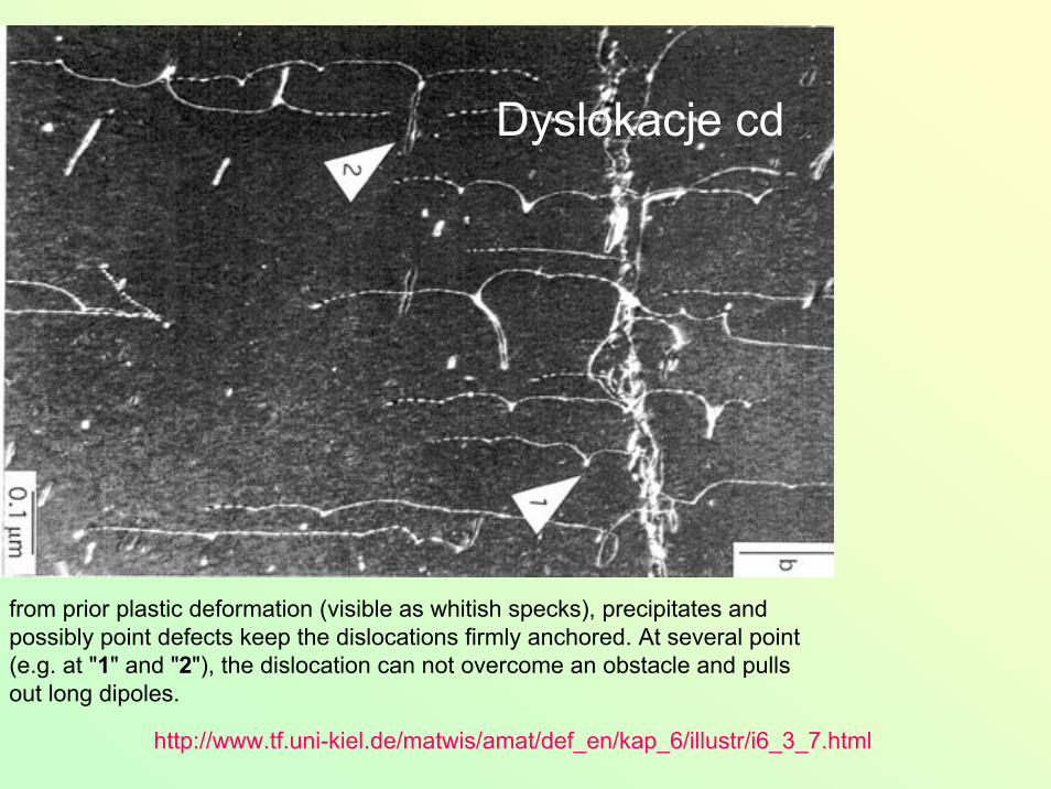
from prior plastic deformation (visible as whitish specks), precipitates and possibly point defects keep the dislocations firmly anchored. At several point (e.g. at "1" and "2"), the dislocation can not overcome an obstacle and pulls out long dipoles.
Dyslokacje cd
http://www.tf.uni-kiel.de/matwis/amat/def_en/kap_6/illustr/i6_3_7.html
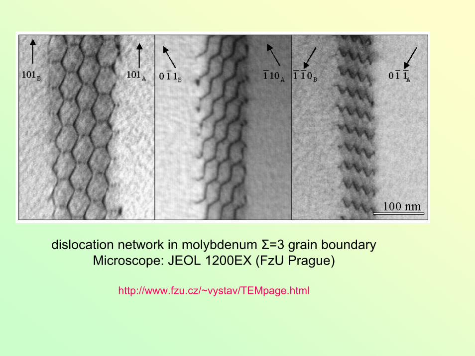
dislocation network in molybdenum Σ=3 grain boundaryMicroscope: JEOL 1200EX (FzU Prague)
http://www.fzu.cz/~vystav/TEMpage.html
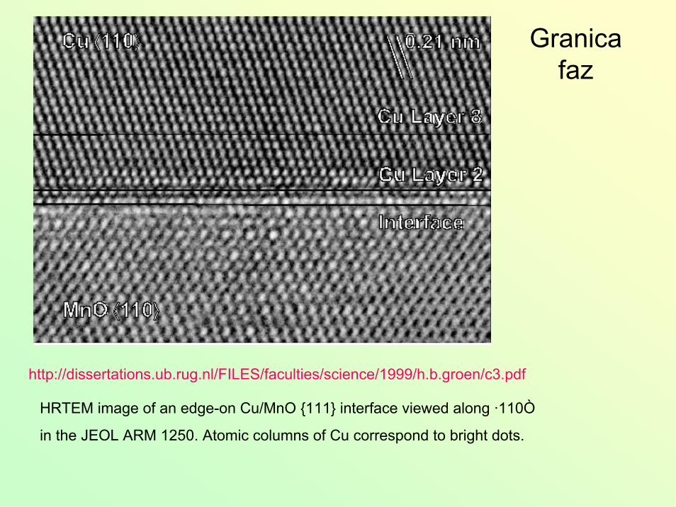
Granica faz
http://dissertations.ub.rug.nl/FILES/faculties/science/1999/h.b.groen/c3.pdf
HRTEM image of an edge-on Cu/MnO {111} interface viewed along ·110Ò
in the JEOL ARM 1250. Atomic columns of Cu correspond to bright dots.
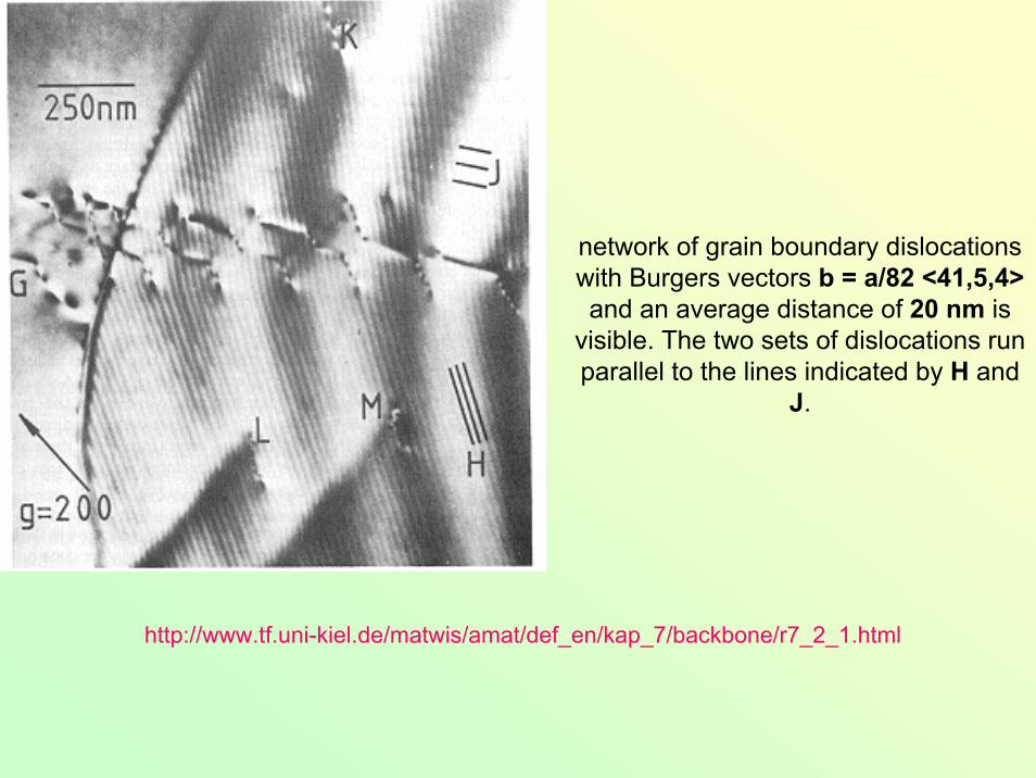
network of grain boundary dislocations with Burgers vectors b = a/82 <41,5,4>and an average distance of 20 nm is
visible. The two sets of dislocations runparallel to the lines indicated by H and
J.
http://www.tf.uni-kiel.de/matwis/amat/def_en/kap_7/backbone/r7_2_1.html
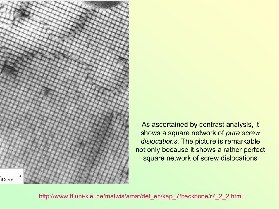
As ascertained by contrast analysis, it shows a square network of pure screw dislocations. The picture is remarkable
not only because it shows a rather perfect square network of screw dislocations
http://www.tf.uni-kiel.de/matwis/amat/def_en/kap_7/backbone/r7_2_2.html
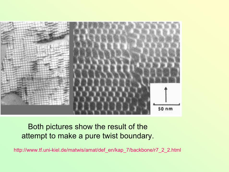
Both pictures show the result of theattempt to make a pure twist boundary.
http://www.tf.uni-kiel.de/matwis/amat/def_en/kap_7/backbone/r7_2_2.html
![A 3)1, î> · teorii funkcjonałów gęstości, określanej skrótem DFT (od nazwy angielskiej: Density Functional Theory) [4-10]. W tej teorii gęstość elektronowa, q (r), zdefiniowana](https://static.fdocuments.pl/doc/165x107/6071f34cf5588609b16972fe/a-31-teorii-funkcjonaw-gstoci-okrelanej-skrtem-dft-od-nazwy.jpg)