
COMBI-Modul 167 phyPS 404 · 2016-12-07 · COMBI-Modul 167 – phyPS-404 PHYTEC Meßtechnik GmbH...
58
A product of a PHYTEC Technology Holding company k i h d C h l i ldi AG COMBI-Modul 167 phyPS 404 Hardware Manual Edition April 2002
Transcript of COMBI-Modul 167 phyPS 404 · 2016-12-07 · COMBI-Modul 167 – phyPS-404 PHYTEC Meßtechnik GmbH...
A product of a PHYTEC Technology Holding companyk i h d C h l i ldi AG
COMBI-Modul 167phyPS 404
Hardware Manual
Edition April 2002
COMBI-Modul 167 – phyPS-404
PHYTEC Meßtechnik GmbH 2002 L-540e_2
In this manual are descriptions for copyrighted products that are not explicitlyindicated as such. The absence of the trademark () and copyright () symbolsdoes not imply that a product is not protected. Additionally, registered patents andtrademarks are similarly not expressly indicated in this manual.
The information in this document has been carefully checked and is believed to beentirely reliable. However, PHYTEC Meßtechnik GmbH assumes noresponsibility for any inaccuracies. PHYTEC Meßtechnik GmbH neither gives anyguarantee nor accepts any liability whatsoever for consequential damages resultingfrom the use of this manual or its associated product. PHYTEC MeßtechnikGmbH reserves the right to alter the information contained herein without priornotification and accepts no responsibility for any damages which might result.
Additionally, PHYTEC Meßtechnik GmbH offers no guarantee nor accepts anyliability for damages arising from the improper usage or improper installation ofthe hardware or software. PHYTEC Meßtechnik GmbH further reserves the rightto alter the layout and/or design of the hardware without prior notification andaccepts no liability for doing so.
Copyright 2002 PHYTEC Meßtechnik GmbH, D-55129 MainzRights - including those of translation, reprint, broadcast, photomechanical orsimilar reproduction and storage or processing in computer systems, in whole or inpart - are reserved. No reproduction may occur without the express writtenconsent from PHYTEC Meßtechnik GmbH.
EUROPE NORTH AMERICA
Address: PHYTEC Technologie Holding AGRobert-Koch-Str. 39D-55129 MainzGERMANY
PHYTEC America LLC255 Ericksen Avenue NEBainbridge Island, WA 98110USA
OrderingInformation:
+49 (800) [email protected]
1 (800) [email protected]
TechnicalSupport:
+49 (6131) [email protected]
1 (800) [email protected]
Fax: +49 (6131) 9221-33 1 (206) 780-9135
Web Site: http://www.phytec.de http://www.phytec.com
2nd Edition April 2002
Inhalt
PHYTEC Meßtechnik GmbH 2002 L-540e_2
Preface...........................................................................................................11 Introduction to the COMBI-Modul 167 ............................................3
1.1 Overview.......................................................................................3
1.2 Block Diagram..............................................................................5
1.3 Software Development Tools .......................................................7
2 Components on the COMBI-Modul 167 ...........................................92.1 Power Supply................................................................................9
2.2 Digital Inputs and Outputs..........................................................10
2.2.1 24 V-Inputs IN0..IN23...................................................10
2.2.2 Relay Outputs ................................................................12
2.2.3 24 V-Outputs .................................................................13
2.2.4 PWM Outputs ................................................................15
2.3 Analog Inputs and Outputs .........................................................16
2.3.1 Analog Inputs ................................................................16
2.3.2 Analog Outputs..............................................................17
2.4 I²C Bus........................................................................................18
2.4.1 Real-Time Clock (RTC) ................................................18
2.4.2 I²C EEPROM.................................................................19
2.4.3 Temperature Sensor.......................................................20
2.5 Interfaces on the COMBI-Modul 167 ........................................21
2.5.1 CAN Interface ...............................................................21
2.5.2 First RS-232 Interface ...................................................22
2.5.3 Second RS-232 Interface...............................................22
2.6 Display and Control Units ..........................................................23
2.6.1 HEX-Encoding Switches S301, S302 ...........................23
2.6.2 DIP Switch S300 ...........................................................24
2.6.3 RUN/STOP Switch........................................................25
2.6.4 Status LEDs ...................................................................25
2.7 Other Components ......................................................................26
2.7.1 RESET...........................................................................26
2.7.2 Jumper Configuration....................................................26
2.7.3 Battery............................................................................27
2.7.4 Expansion Connector.....................................................28
2.8 Port Assignment Summary .........................................................29

COMBI-Modul 167 – phyPS-404
PHYTEC Meßtechnik GmbH 2002 L-540e_2
3 Memory Models................................................................................. 353.1 Memory Configuration............................................................... 35
3.1.1 Chip Select Signals........................................................ 35
3.1.2 Chip Select Signal for CODE Flash U4/5..................... 38
3.1.3 Chip Select Signal for SRAM U6/7 .............................. 39
3.1.4 Chip Select Signal for DATA Flash U2/3..................... 40
3.1.5 Chip Select Signal for External UART......................... 41
3.1.6 Chip Select Signal /CS4 ................................................ 42
4 Hints for Installing the COMBI-Modul 167 ................................... 435 Hints for Operating the COMBI-Modul 167.................................. 446 Technical Specifications.................................................................... 45Index............................................................................................................ 49
Index of Figures
Figure 1: Block Diagram COMBI-Modul 167 ............................................ 5
Figure 2: View of the COMBI-Modul 167 (Top Side)................................ 6
Figure 3: Location of the Function Blocks .................................................. 7
Figure 4: Connecting a Power Supply ......................................................... 9
Figure 5: Circuitry on the 24 V-Inputs....................................................... 10
Figure 6: Input Circuitry Options............................................................... 11
Figure 7: Relay Output Circuitry ............................................................... 12
Figure 8: 24 V-Outputs Circuitry............................................................... 13
Figure 9: PWM Outputs Circuitry.............................................................. 15
Figure 10: Analog Inputs Circuitry.............................................................. 16
Figure 11: Analog Outputs Circuitry ........................................................... 17
Figure 12: HEX-Encoding Switches S301, S302 ........................................ 23
Figure 13: DIP-Switch S300........................................................................ 24
Figure 14: Memory Configuration Example................................................ 36
Inhalt
PHYTEC Meßtechnik GmbH 2002 L-540e_2
Index of Tables
Table 1: I/O Port Arrangement of the 24 V-Inputs...................................10
Table 2: Function and I/O Port Arrangement of Relay Outputs ...............12
Table 3: Function and I/O Port Arrangement of 24 V-Outputs ................14
Table 4: Accessing the Error Detection State of the 24 V-Outputs..........14
Table 5: LEDs for Output State Control ...................................................14
Table 6: Function and I/O Port Arrangement of PWM Outputs...............15
Table 7: Function and I/O Port Arrangement of Analog Inputs ...............16
Table 8: Function and I/O Port Arrangement of Analog Outputs ............17
Table 9: RTC Address ..............................................................................19
Table 10: I²C EEPROM Address................................................................19
Table 11: I²C Temperature Sensor Address................................................20
Table 12: Example Values for CAN Cable Parameters..............................21
Table 13: First RS-232 Pin Assignment .....................................................22
Table 14: Optional Second RS-232 Pin Assignment at JPRS-232.............22
Table 15: Function and I/O Port Arrangement of theHEX-Encoding Switches............................................................23
Table 16: Function and Data Line Arrangement of the DIP Switch...........24
Table 17: Encoding the RUN/STOP Switch S303 Positions......................25
Table 18: Example for Using the Status LED's ..........................................25
Table 19: Expansion Connector Pin Assignment .......................................28
Table 20: Connector Pin Assignment COMBI-Modul 167(Upper Row) ...............................................................................30
Table 21: Connector Pin Assignment COMBI-Modul 167(Lower Row)...............................................................................31
Table 22: Port Pin Assignment for I2C Bus, RTC Interrupt andHEX-Encoding Switch ...............................................................32
Table 23: Port Pin Assignment for RUN/STOP Switch, Status LEDs,S300 and Second Serial Interface...............................................32
Table 24: Port Pin Assignment for External Connections..........................33

COMBI-Modul 167 – phyPS-404
PHYTEC Meßtechnik GmbH 2002 L-540e_2
Table 25: Standard Assignment for /CS Signals ........................................ 35
Table 26: /CS0 Configuration for CODE Flash ......................................... 38
Table 27: Address Range with 256 kByte CODE Flash............................. 38
Table 28: /CS2 Configuration for SRAM................................................... 39
Table 29: Address Range with 256 kByte SRAM...................................... 39
Table 30: /CS1 Configuration for DATA Flash ......................................... 40
Table 31: /CS3 Configuration for External UART .................................... 41
Table 32: Functions of Chip Select Signal /CS4 ........................................ 42
Table 33: /CS4 Configuration..................................................................... 42
Table 34: Technical Data 24 V-Inputs ....................................................... 45
Table 35: Technical Data Relay Inputs ...................................................... 46
Table 36: Technical Data 24 V-Outputs..................................................... 46
Table 37: Technical Data Analog Inputs .................................................... 47
Table 38: Technical Data Analog Outputs ................................................. 47
Preface
PHYTEC Meßtechnik GmbH 2002 L-540e_2 1
Preface
This COMBI-Modul 167 Hardware Manual describes the board’sdesign and functions. Precise specifications for the Infineon C167CRmicrocontroller can be found in the enclosed microcontroller DataSheet/User’s Manual. If software is included please also refer toadditional documentation for this software.
In this hardware manual and in the attached schematics, low activesignals are denoted by a "/" in front of the signal name (i.e.: /RD). A"0" indicates a logic-zero or low-level signal, while a "1" represents alogic-one or high-level signal.
The following manuals are available for additional information:
Installation and Getting Started Guide
• describes the initial installation steps for this control unit andprovides QuickStart instruction on how to get the device up andrunning with an existing example program
Infineon C167CR User’s Manual / Data Sheet
• describes the features and functions of the C167CR micro-controller in detail
Module Software Drivers
• describes the accompanying software driver functions foraccessing the COMBI-Modul 167 function components anddemonstrates their use with an example program
Example circuitry shown in this manual is provided as generalcircuitry examples and do not necessarily reflect the actual circuitdesign. The exact circuitry is provided in the schematics includedwith the COMBI-Modul 167.

COMBI-Modul 167 – phyPS-404
2 PHYTEC Meßtechnik GmbH 2002 L-540e_2

Introduction
PHYTEC Meßtechnik GmbH 2002 L-540e_2 3
1 Introduction to the COMBI-Modul 167
1.1 Overview
The COMBI-Modul 167 is a compact control system for universalprocessing purposes of standard industrial signals. The board isdesigned for a great variety of uses, such as main control unit inmeasurement, control and data processing applications. TheCOMBI-Modul 167 is also an ideal solution in distributed field bussystems in conjunction with other components and systems of theIGAS-(Integrated Automation System) product series.
The COMBI-Modul design is primarily based on the provenPHYTEC microcontroller core boards and makes use of the InfineonC167 microcontroller resources. Most of the microcontroller’s I/Oports are interrupt capable, thus enabling very short response times.
Peripheral sensors, actuators and control devices can be easilyconnected to the board using lug connector strips. Use of stable,removable screw thimbles (f.e. COMBICON) enables easy exchangeof the connected sensors and actuators. The board is installed in anindustry proven PHOENIX casing and can be mounted on a DIN/ENchassis bar.
The COMBI-Modul 167 is populated with 256 kByte (up to 1 MBoptional) static RAM (battery buffered) and 256 kByte (up to2 MB optional) Flash memory. The board offer serial RS-232interfaces for connection to terminals or programming devices. TheCOMBI-Modul 167 also features an optically isolated CAN(Controller Area Network) field bus interface and a battery-bufferedReal-Time Clock (RTC).
COMBI-Modul 167 – phyPS-404
4 PHYTEC Meßtechnik GmbH 2002 L-540e_2
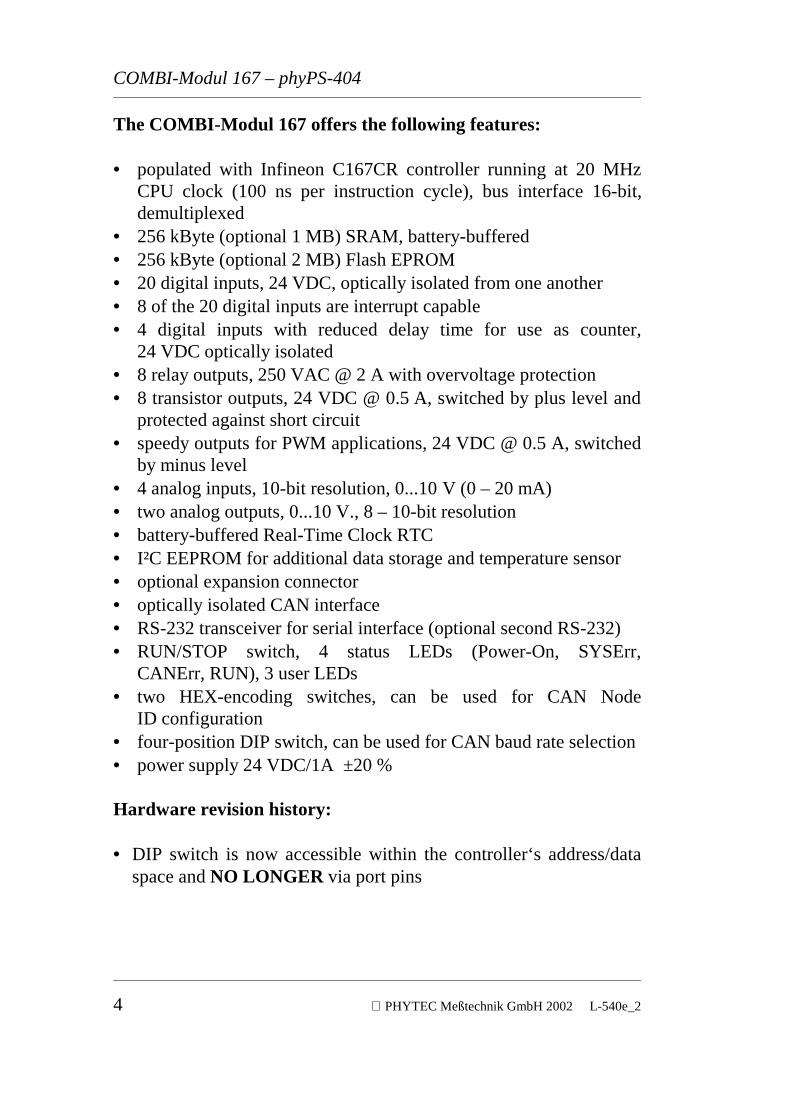
The COMBI-Modul 167 offers the following features:
• populated with Infineon C167CR controller running at 20 MHzCPU clock (100 ns per instruction cycle), bus interface 16-bit,demultiplexed
• 256 kByte (optional 1 MB) SRAM, battery-buffered• 256 kByte (optional 2 MB) Flash EPROM• 20 digital inputs, 24 VDC, optically isolated from one another• 8 of the 20 digital inputs are interrupt capable• 4 digital inputs with reduced delay time for use as counter,
24 VDC optically isolated• 8 relay outputs, 250 VAC @ 2 A with overvoltage protection• 8 transistor outputs, 24 VDC @ 0.5 A, switched by plus level and
protected against short circuit• speedy outputs for PWM applications, 24 VDC @ 0.5 A, switched
by minus level• 4 analog inputs, 10-bit resolution, 0...10 V (0 – 20 mA)• two analog outputs, 0...10 V., 8 – 10-bit resolution• battery-buffered Real-Time Clock RTC• I²C EEPROM for additional data storage and temperature sensor• optional expansion connector• optically isolated CAN interface• RS-232 transceiver for serial interface (optional second RS-232)• RUN/STOP switch, 4 status LEDs (Power-On, SYSErr,
CANErr, RUN), 3 user LEDs• two HEX-encoding switches, can be used for CAN Node
ID configuration• four-position DIP switch, can be used for CAN baud rate selection• power supply 24 VDC/1A ±20 %
Hardware revision history:
• DIP switch is now accessible within the controller‘s address/dataspace and NO LONGER via port pins
Introduction
PHYTEC Meßtechnik GmbH 2002 L-540e_2 5
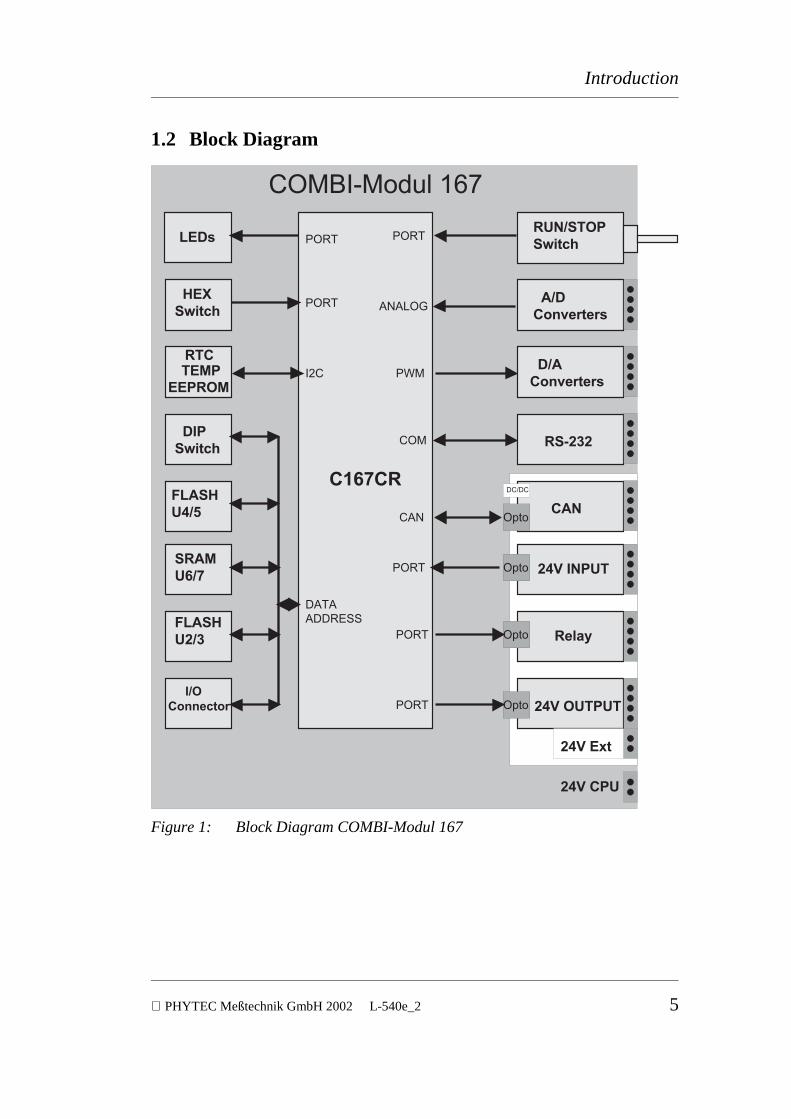
1.2 Block Diagram
RTCTEMP
EEPROM
DIPSwitch
HEXSwitch
LEDs
FLASHU4/5
SRAMU6/7
FLASHU2/3
I/OConnector
RUN/STOPSwitch
A/DConverters
D/AConverters
RS-232
CAN
24V INPUT
Relay
24V OUTPUT
24V Ext
24V CPU
DC/DC
Opto
Opto
Opto
Opto
C167CR
PORT
I2C
PORT PORT
PORT
PORT
PORT
DATAADDRESS
CAN
COM
PWM
ANALOG
COMBI-Modul 167
Figure 1: Block Diagram COMBI-Modul 167
COMBI-Modul 167 – phyPS-404
6 PHYTEC Meßtechnik GmbH 2002 L-540e_2
RELAY
RELAY
RELAY
RELAY
RELAY
RELAY
RELAY
RELAY
OUT8
OUT9
OUT10
OUT11
OUT12
OUT13
OUT14
OUT15
OUT7
OUT6
OUT5
OUT4
OUT2
OUT1
OUT0
OUT3
BATTERY
IN16
IN17
IN18
IN19
IN20
IN21
IN22
IN23
IN8
IN9
IN10
IN11
IN12
IN13
IN14
IN15
IN0
IN1
IN2
IN3
IN4
IN5
IN6
IN7
AIN3
AIN1
AIN2
AIN0
AOUT0
AOUT1
PE
24V-CPU
RUN/STOP
IO-Connector
SYSERR
ERROR
RUN
POWER
JP300
RESET
S300/S
301/S
302
PE
24VDC Ext.
OUT16
OUT17
RS-232
CAN
FLASHU4FLASHU4
FLASHU5
SRAM U6
Controller
CGNDCANLCANH
RxDGNDTxD
2. RS-232
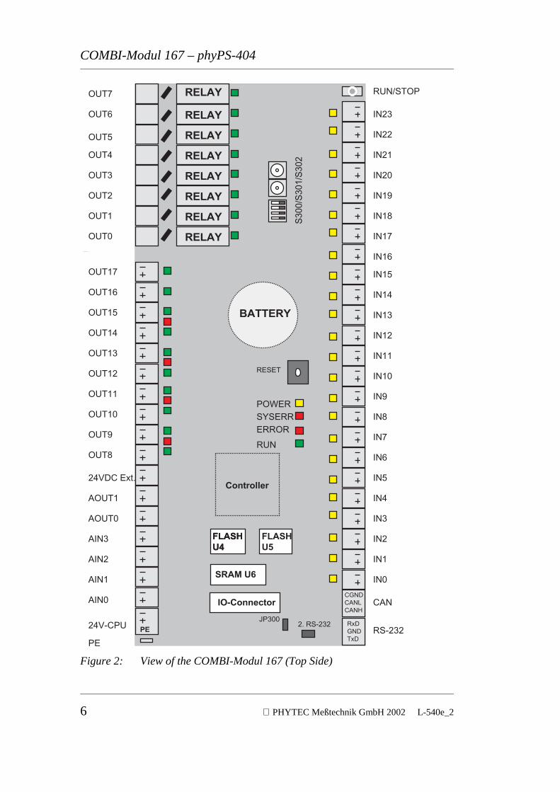
Figure 2: View of the COMBI-Modul 167 (Top Side)
Introduction
PHYTEC Meßtechnik GmbH 2002 L-540e_2 7
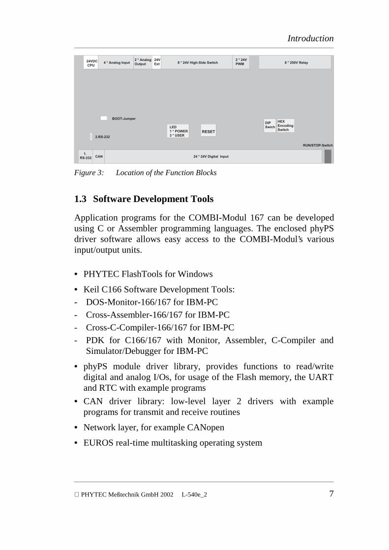
24VDC CPU
4 * Analog Input2 * Analog Output
24VExt 8 * 24V High-Side Switch
2 * 24VPWM 8 * 250V Relay
BOOT-Jumper
LED1 * POWER3 * USER
RESET
DIPSwich
HEX EncodingSwitch
RUN/STOP-Switch
24 * 24V Digital InputCAN 1.RS-232
2.RS-232
Figure 3: Location of the Function Blocks
1.3 Software Development Tools
Application programs for the COMBI-Modul 167 can be developedusing C or Assembler programming languages. The enclosed phyPSdriver software allows easy access to the COMBI-Modul’s variousinput/output units.
• PHYTEC FlashTools for Windows
• Keil C166 Software Development Tools:- DOS-Monitor-166/167 for IBM-PC- Cross-Assembler-166/167 for IBM-PC- Cross-C-Compiler-166/167 for IBM-PC- PDK for C166/167 with Monitor, Assembler, C-Compiler and
Simulator/Debugger for IBM-PC
• phyPS module driver library, provides functions to read/writedigital and analog I/Os, for usage of the Flash memory, the UARTand RTC with example programs
• CAN driver library: low-level layer 2 drivers with exampleprograms for transmit and receive routines
• Network layer, for example CANopen
• EUROS real-time multitasking operating system

COMBI-Modul 167 – phyPS-404
8 PHYTEC Meßtechnik GmbH 2002 L-540e_2

Components on the COMBI-Modul 167
PHYTEC Meßtechnik GmbH 2002 L-540e_2 9
2 Components on the COMBI-Modul 167
2.1 Power Supply
The COMBI-Modul 167 features two galvanic isolated power supplyinputs.
The power supply input 24 VDC-CPU supplies the microcontroller,the core circuitry and the relay on the COMBI-Modul 167.A DC voltage power source in the range of 24 V +/-20 % can beconnected to this input. The typical current draw is 80..100 mA.
The power supply input 24 VDC-Ext. supplies the transistor outputs(OUT8..15) and the PWM outputs (OUT16..17). A DC voltage powersource in the range of 24 V +/-20 %, can be connected to this input.The current draw depends on the power consumption of the devicesconnected to the transistor outputs. The maximum current draw isspecified with 4 A.
Figure 4: Connecting a Power Supply
Power supply inputs are protected against polarity reversal in eachcase by a diode in the positive voltage input. Do not connect powersupply connections to analog inputs or outputs as this could destroythe analog circuitry.
The flat connector next to the 24 VDC-CPU connection serves as aPE-connector. The flat connector must be connected to protect earth(PE) potential with a short cable that is able to carry high currentspikes.
24VDCCPU
4 * Analog Input 2* Analog Output
24VExt.
PE + - + -
24VDC Power Supply
+ 24V GND
PE-Connector

COMBI-Modul 167 – phyPS-404
10 PHYTEC Meßtechnik GmbH 2002 L-540e_2
2.2 Digital Inputs and Outputs
2.2.1 24 V-Inputs IN0..IN23
VCC
+
-
PORTOpto-Coupler
Figure 5: Circuitry on the 24 V-Inputs
The COMBI-Modul 167 provides a maximum of 24 digital inputs thatare directly routed to the C167CR microcontroller port pins. Therelation of inputs to port pins is shown in Table 1.
The inputs labeled as IN8..IN15 can also serve as interrupt inputs.Furthermore, IN20...IN23 can be used as fast timer inputs, with amaximum input frequency of 50 kHz.
Input Label Port Special FunctionIN8..IN15 P2.8...P2.15 Interrupt inputIN0-IN7
IN16..IN19P2.0...P2.7P5.4...P5.7
-
IN20..IN21IN22..IN23
P3.5,P3.6P5.12,P5.13
Timer input
Table 1: I/O Port Arrangement of the 24V Inputs

Components on the COMBI-Modul 167
PHYTEC Meßtechnik GmbH 2002 L-540e_2 11
All digital inputs IN0..IN23 are active low with the followingswitching voltages:
• Input voltage > 13 VDC: ‘0’ (TTL level) on port pin• Input voltage < 5 VDC: ‘1’ (TTL level) on port pin
The inputs are separated from one another and from the controllercore via an opto-coupler. Since the inputs themselves arepotential-free, they can be turned on by the 24 VDC or the24 VDC-GND. The following figure illustrates two connectionpossibilities for digital inputs:
24VDC 24VDC
Low-SideInput
High-SideInput
Figure 6: Input Circuitry Options
COMBI-Modul 167 – phyPS-404
12 PHYTEC Meßtechnik GmbH 2002 L-540e_2
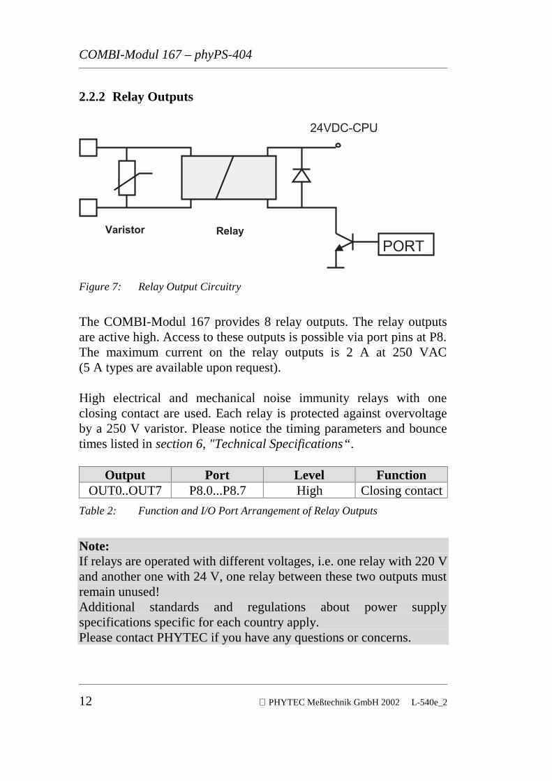
2.2.2 Relay Outputs
24VDC-CPU
PORTVaristor Relay
Figure 7: Relay Output Circuitry
The COMBI-Modul 167 provides 8 relay outputs. The relay outputsare active high. Access to these outputs is possible via port pins at P8.The maximum current on the relay outputs is 2 A at 250 VAC(5 A types are available upon request).
High electrical and mechanical noise immunity relays with oneclosing contact are used. Each relay is protected against overvoltageby a 250 V varistor. Please notice the timing parameters and bouncetimes listed in section 6, "Technical Specifications“ .
Output Port Level FunctionOUT0..OUT7 P8.0...P8.7 High Closing contact
Table 2: Function and I/O Port Arrangement of Relay Outputs
Note:If relays are operated with different voltages, i.e. one relay with 220 Vand another one with 24 V, one relay between these two outputs mustremain unused!Additional standards and regulations about power supplyspecifications specific for each country apply.Please contact PHYTEC if you have any questions or concerns.

Components on the COMBI-Modul 167
PHYTEC Meßtechnik GmbH 2002 L-540e_2 13
2.2.3 24 V-Outputs
VCC
+
-
Status 8/9Opto-Coupler
VCCOpto-Coupler
PORT
VCC
Logic and Protection Circuit
IOVCC
24V Ext.
Figure 8: 24 V-Outputs Circuitry
The COMBI-Modul 167 provides 8 outputs for 24 V digital signals.These outputs are active low and protected against short circuit. Theswitching time is 400µs. The maximum current on the 24 V-Outputsis 0.5 A. The sum of the current load on all outputs OUT8..OUT17must not exceed 4 A.
The 24 V-Outputs provide an error detection functionality for shortcircuits (higher than 1.5....2 A) at outputs OUT8/9, OUT10/11,OUT12/13 and OUT14/15. A red error LED will illuminate in case ofa short circuit. The state of the LED is accessible by read instructionsand can be reset with the controller’s Chip Select signal /CS4. Signalsare routed through an opto-coupler for galvanic isolation. Any shortcircuit is indicated by a low level signal. The state output of thetransistor is not static, but the transistor tries to turn on again after acertain period of time. This will automatically switch the status levelback to high.
COMBI-Modul 167 – phyPS-404
14 PHYTEC Meßtechnik GmbH 2002 L-540e_2
For this reason, each short circuit that occurs is stored in the circuitryuntil the user program resets the status. Resetting the four statussignals is done with an /RD access to the Chip Select signal’s /CS4base address 03H. Following a reset or power-on, the status levelmust be reset in order to initialize the error detection circuitry andprovide known signal levels. It is possible that circuitry may be set toerror state, even if a short circuit did not occur.
The user should also note, that any short circuit is detected with adelay time of 1 ms to 5 ms after the output is set.
Output Port Switch Function CommentsOUT8..OUT11 P3.0...P3.3 24 V high-side
switchshort circuitprotected
OUT12..OUT15 P7.4...P7.7 24 V high-sideswitch
short circuitprotected
Table 3: Function and I/O Port Arrangement of 24 V-Outputs
/CS4 BaseAddress plus
Data Bit Error State at... Signal ActiveLevel
2 D0..D3 OUT8/9...OUT14/15 Low3 Reset state with /RD access
Table 4: Accessing the Error Detection State of the 24 V-Outputs
Controlled Output Pair LED (red)OUT8/9 D832OUT10/11 D833OUT12/13 D834OUT14/15 D835
Table 5: LEDs for Output State Control
Note:The BTS712 integrated circuit has been discontinued afterfinalization of the COMBI Modul-167’s design. The BTS712 will beused as replacement part on all devices assembled after year 2001.This also results in a change of the state indication function. The stateoutput will indicate "Open Load" state if the output load current islower than 100 mA at room temperature.

Components on the COMBI-Modul 167
PHYTEC Meßtechnik GmbH 2002 L-540e_2 15
2.2.4 PWM Outputs
+
-
VCCOpto-Coupler
PORT
24V Ext.
IOVCC
Figure 9: PWM Outputs Circuitry
The COMBI-Modul 167 provides two PWM outputs OUT16 andOUT17. These outputs are active low and controlled via the controllerports P7.0 = OUT16 and P7.1 = OUT17. These outputs switch theGround potential when activated, therefore the load must beconnected to the 24 V supply.
The maximum current load on the PWM outputs is 0.5 A for eachchannel. The sum of the current load on all outputs OUT8..OUT17must not exceed 4 A.
Output Port Switch Function MaximumFrequency
OUT16OUT17
P7.0P7.1
24 V low-sideswitch
50 kHz
Table 6: Function and I/O Port Arrangement of PWM Outputs
COMBI-Modul 167 – phyPS-404
16 PHYTEC Meßtechnik GmbH 2002 L-540e_2
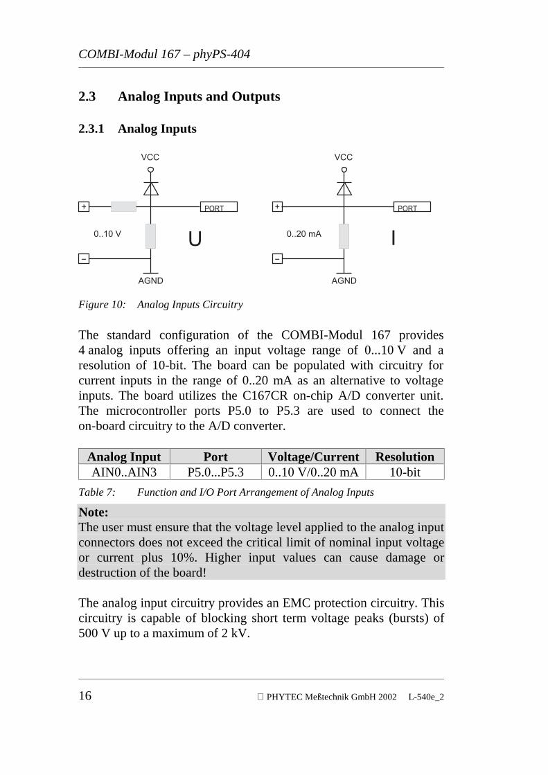
2.3 Analog Inputs and Outputs
2.3.1 Analog Inputs
+
-
VCC
PORT
AGND
+
-
VCC
PORT
AGND
0..10 V 0..20 mAU I
Figure 10: Analog Inputs Circuitry
The standard configuration of the COMBI-Modul 167 provides4 analog inputs offering an input voltage range of 0...10 V and aresolution of 10-bit. The board can be populated with circuitry forcurrent inputs in the range of 0..20 mA as an alternative to voltageinputs. The board utilizes the C167CR on-chip A/D converter unit.The microcontroller ports P5.0 to P5.3 are used to connect theon-board circuitry to the A/D converter.
Analog Input Port Voltage/Current ResolutionAIN0..AIN3 P5.0...P5.3 0..10 V/0..20 mA 10-bit
Table 7: Function and I/O Port Arrangement of Analog Inputs
Note:The user must ensure that the voltage level applied to the analog inputconnectors does not exceed the critical limit of nominal input voltageor current plus 10%. Higher input values can cause damage ordestruction of the board!
The analog input circuitry provides an EMC protection circuitry. Thiscircuitry is capable of blocking short term voltage peaks (bursts) of500 V up to a maximum of 2 kV.
Components on the COMBI-Modul 167
PHYTEC Meßtechnik GmbH 2002 L-540e_2 17
2.3.2 Analog Outputs
REF
PWM
AGND
+
-
Low-Pass
0..10 V
Figure 11: Analog Outputs Circuitry
Two analog output signals can be generated on theCOMBI-Modul 167. The C167CR microcontroller provides aCompare/Capture unit that allows generation of pulse widthmodulated (PWM) signals at ports P7.2 and P7.3. The on-boardcircuitry, with an active low-pass and operational amplifier, supportsanalog output signals in the range of 0...10 V with a resolution of8-bit and an accuracy of ±1 %. A higher D/A resolution is possible,however this reduces the accuracy of the output voltage, since theaccuracy depends on the chosen base frequency and therefore theresolution of the PWM signal.
Analog Output Port Voltage ResolutionAOUT0AOUT1
P7.2P7.3
0..10 V 8-bit
Table 8: Function and I/O Port Arrangement of Analog Outputs

COMBI-Modul 167 – phyPS-404
18 PHYTEC Meßtechnik GmbH 2002 L-540e_2
2.4 I²C Bus
The I2C bus is realized via port pins P3.8 = SendData (SDA) andP3.9 = SendClock (SCL). The I2C bus protocol is implemented infirmware.
2.4.1 Real-Time Clock (RTC)
For real-time or time-driven applications, the COMBI-Modul 167 isequipped with an RTC-8583 Real-Time Clock. This RTC deviceprovides the following features:
• Serial input/output bus (I2C)• Power consumption
Bus inactive, CLKOUT = 0 kHz : max. 50 µA• Clock function with four year calendar• Century bit for year 2000-compliance• Universal timer with alarm and overflow indication• 24-hour format• Automatic word address incrementing• Programmable alarm, timer and interrupt functions
If the COMBI-Modul 167 is equipped with a battery, the Real-TimeClock runs independently of the board’s power supply (refer tosection 2.7.3, "Battery").
Programming the Real-Time Clock is done via the I2C bus(address 1010001B), which is connected to port P3.9 (SCL) and portP3.8 (SDA). The Real-Time Clock also provides an interrupt outputthat extends to port P3.7. An interrupt occurs in the event of a clockalarm, timer alarm, timer overflow and event counter alarm. Aninterrupt must be cleared by software. The Real-Time Clock can beutilized in various applications. For more information on the featuresof the RTC-8583, refer to the corresponding Data Sheet.

Components on the COMBI-Modul 167
PHYTEC Meßtechnik GmbH 2002 L-540e_2 19
Note:After connection of the supply voltage, or after a hardware reset, theReal-Time Clock generates no interrupt. The RTC must first beinitialized (see RTC Data Sheet for more information)
I²C software drivers and demo programs are included on the tool diskor CD-ROM.
I²C Device I²C AddressRTC 1010001B
Table 9: RTC Address
2.4.2 I²C EEPROM
The COMBI-Modul 167 can be equipped with an I²C EEPROM.Data, which has to be maintained even if a power supply is notconnected to the COMBI-Modul 167, can be stored in theI²C EEPROM. The standard I²C EEPROM memory size is 8 kBytes,however it is also possible to populate different size EEPROMdevices on the board. The I²C EEPROM is self-protect(via Jumper JP200) from overwriting (optional).
Programming the I²C EEPROM is done via the I2C bus(address 1010011B), which is connected to port P3.9 (SCL) and portP3.8 (SDA). For more information on the features of theI²C EEPROM, refer to the corresponding Data Sheet.
I²C Device I²C AddressEEPROM 1010011B
Table 10: I²C EEPROM Address

COMBI-Modul 167 – phyPS-404
20 PHYTEC Meßtechnik GmbH 2002 L-540e_2
2.4.3 Temperature Sensor
The COMBI-Modul 167 can be equipped with an optionaltemperature sensor at U205. The I2C bus also controls this componentat address 1001111B. The sensor is located next to the battery holder.For more information on the features of the I²C temperature sensor,refer to the corresponding Data Sheet.
The temperature sensor has the following features:
• measurement of temperature in the range of –25...+100°C(+/-3°C)
• adjustable threshold for exceeding temperature limit with interruptsignal
I²C Device I²C AddressTemperature Sensor 1001111B
Table 11: I²C Temperature Sensor Address

Components on the COMBI-Modul 167
PHYTEC Meßtechnik GmbH 2002 L-540e_2 21
2.5 Interfaces on the COMBI-Modul 167
2.5.1 CAN Interface
The C167CR microcontroller is equipped with an integratedFULL-CAN interface. The signals CAN_HIGH, CAN_LOW andCAN_GND are galvanically decoupled and assessable on theCOMBICON connectors. An external power supply is not required.Information about the CAN interface can be found in the C167CRUser’s Manual/Data Sheet.
The CAN bus cable can be either a twisted pair or a ribbon cable. Thecable has to be terminated with a resistor of 120 Ohm betweenCAN_H and CAN_L at both ends of the bus cable. The cableshielding should be connected to PE at both ends of the cable. Thewave resistance of the cable should be 120 Ohm. The connectionbetween the cable length and the usable CAN bitrate is shown in thetable below. These values are approximate values, exact cableparameters must be calculated using the appropriate formulas. It isrecommended to optically isolate the CAN nodes for cable extensionsof more than 200 meters.
Cable Length [m] Maximum Bitrate [kBit/s]0 ... 25 10000 ...100 5000 ....250 2500 ... 500 1250 ...2500 20
Table 12: Example Values for CAN Cable Parameters
The Philips P82C251 is used as a CAN transceiver. This devicesupports up to 100 nodes on one CAN bus with a maximum bitrate of1 MBit/s.
COMBI-Modul 167 – phyPS-404
22 PHYTEC Meßtechnik GmbH 2002 L-540e_2
2.5.2 First RS-232 Interface
The internal serial interface of the C167CR controller is used for thefirst RS-232 interface on the COMBI-Modul 167.
This interface is primarily used for communication with PHYTECFlashTools for program download or for debugging with thecorresponding monitor program. The RS-232 level signals RxD, TxDand GND are available at the COMBICON connectors. A shieldedserial cable should be used for connecting the board to a host-PC. Theshield needs to be connected to PE on one side of the cable in order toensure proper functioning.
Pin # RS-232 Signals1 TxD2 GND3 RxD
Table 13: First RS-232 Pin Assignment
2.5.3 Second RS-232 Interface
The COMBI-Modul 167 can also be equipped with an optionalsecond serial RS-232 interface. The second serial interface is realizedwith the SCC2691 UART chip. Port pin 6.3 of the C167CR controlleris used to generate the Chip Select signal for access to the UART. A3-pin header connector at JPRS-232 (located inside the housing) isprovided for the physical connection. Alternatively, it is possible toroute the second serial interface signals to the COMBICON connectorthat is intended for use as the CAN interface. In the latter case, theCAN interface circuitry must not be mounted on the board.
Pin # atJPRS-232
RS-232 Signals
1 TxD2 RxD3 GND
Table 14: Optional Second RS-232 Pin Assignment at JPRS-232
Components on the COMBI-Modul 167
PHYTEC Meßtechnik GmbH 2002 L-540e_2 23
The address range for the UART /CS signal (/CS3 of the C167CR)can be configured with software (refer to the C167CR User’sManual/Data Sheet). Technical data for the UART chip and theRS-232 transceiver, located at U203, can be found in thecorresponding Data Sheets for these components.
2.6 Display and Control Units
2.6.1 HEX-Encoding Switches S301, S302
The COMBI-Modul 167 is equipped with two HEX encodingswitches on S301 (MSB) and S302 (LSB). Both switches are locatedinside the housing and offer no EMC protection circuitry. The twoHEX encoding switches are intended for configuration purposes priorto operation rather than implementing the switches as a control unitduring runtime.
20 21 22 23
DIP Switch S300
HEX Switch S301
HEX Switch S302
MSB LSB
Figure 12: HEX-Encoding Switches S301, S302
Switch Value Port PinS301 20 P5.11S301 21 P5.10S301 22 P5.9S301 23 P5.8S302 20 P3.13S302 21 P3.15S302 22 P5.15S302 23 P5.14
Table 15: Function and I/O Port Arrangement of the HEX-Encoding Switches

COMBI-Modul 167 – phyPS-404
24 PHYTEC Meßtechnik GmbH 2002 L-540e_2
The HEX-encoding switch signals are active high. Bounce timesduring switching must be considered when implementing softwarefunctions that access the HEX-encoding switch. These switches canbe used for setting up the node address when integrating theCOMBI-Modul 167 into a CAN network.
2.6.2 DIP Switch S300
The COMBI-Modul 167 is equipped with a 4-position DIP switch atS300. The DIP switch is located inside the housing and offers noEMC protection circuitry. The DIP switch is intended forconfiguration purposes prior to operation rather than implementingthe switches as a control unit during runtime.
20 21 22 23
DIP-Switch S300
HEX-Switch S301
HEX-Switch S302
MSB LSB
Figure 13: DIP-Switch S300
The 4-position DIP switch can be accessed at the Chip Select signal/CS4 base address. The switch signals are active high and available atdata lines D0...D3 with read access.
Switch Value Data LineS300 20 D0S300 21 D1S300 22 D2S300 23 D3
Table 16: Function and Data Line Arrangement of the DIP Switch
The bounce times during switching must be considered whenimplementing software functions that access the DIP switch. Theseswitches can be used for configuration of the CAN bitrate whenintegrating the COMBI-Modul 167 into a CAN network.
Components on the COMBI-Modul 167
PHYTEC Meßtechnik GmbH 2002 L-540e_2 25
2.6.3 RUN/STOP Switch
The RUN/STOP switch, located at S303, provides 3 switch positions.The following table gives an example on how to use the switch statesRUN, STOP and MRES.
Switch Position Level at P6.6 Level at P3.4RUN 0 1STOP 1 1MRES 1 0
Table 17: Encoding the RUN/STOP Switch S303 Positions
The RUN/STOP switch on the COMBI-Modul 167 is the only controlunit which is available for use during system runtime. It offers EMCprotection circuitry, which can tolerate voltage bursts up to 2 kV. Thisrequires that the unit is connected to PE via the applicable connector.
The bounce times during switching must be considered whenimplementing software functions that access the RUN/STOP switch.These switches can be used for configuring operational states of thedevice when integrating the COMBI-Modul 167 into a CAN network.
2.6.4 Status LEDs
Three of the four status LEDs are connected to port pins on theC167CR. This allows direct access with the bit-clear and bit-setinstructions. These LEDs are freely available and can be used asrequired by the application. The table below illustrates possibleapplications for the LEDs:
LED Port Pin LED on MeaningD5 (green) P4.4 P4.4 = 0 Program is in ’RUN’ stateD6 (red) P4.7 P4.7 = 0 Network errorD7 (red) P6.5 P6.5 = 0 System errorD8 (yellow) VCC - Power supply is on
Table 18: Example for Using the Status LED’s

COMBI-Modul 167 – phyPS-404
26 PHYTEC Meßtechnik GmbH 2002 L-540e_2
2.7 Other Components
2.7.1 RESET
The COMBI-Modul 167 is equipped with a TLC7705 Resetcontroller. The reset signal is released if the voltage level of thenominal 5 V supply drops below the 4.65 V reset threshold.
The Reset push button S1 (located next to the battery holder) can beused to release a manual Reset of the COMBI-Modul 167. The Resetbutton is located inside the housing and offers no EMC protectioncircuitry. The Reset button is intended for use during the softwaredesign phase, as well as for starting PHYTEC FlashTools on theboard.
Note:When touching the reset push button, electro-static discharges cancause serious damage or even destruction to the COMBI-Modul. Thedevice should be unpacked, handled or operated only in environmentsin which sufficient precautionary measures have been taken.
2.7.2 Jumper Configuration
The Boot jumper JB300 is used to configure the start condition for theon-chip Bootstrap loader. If the insertable jumper JB300 is closed,then the COMBI-Modul 167 will go into Boostrap mode following ahardware reset. This allows PHYTEC FlashTools to start, in order todownload user code into the on-board Flash. If the Boot jumperremains open, then the application code stored in the Flash U4/U5will be executed after Reset.
Additional solder jumpers are also available on theCOMBI-Modul 167. These jumpers are pre-configured according tothe memory configuration of the board at time of delivery and mustnot be changed. Changes of the memory configuration can be madewith software.

Components on the COMBI-Modul 167
PHYTEC Meßtechnik GmbH 2002 L-540e_2 27
2.7.3 Battery
The battery that buffers the memory is not essential to the functioningof the COMBI-Modul 167. However, this battery buffer embodies aneconomical and practical means of storing non-volatile data inSRAM. It is also necessary for data storage in the Real-Time Clock inthe event of a power failure. A battery is installed in the battery socketon the board at time of delivery.
Power consumption depends on the installed memory devices andtheir capacity. The typical current draw for memory chips used on theCOMBI-Modul 167 is 1 µA (max. 100 µA) for each RAM device.The RTC typically draws 5 µA (max. 50 µA). The standard version ofthe board has a typical data retention time of one year when the powersupply (24 V CPU) is disconnected.
Exchanging the battery yearly is highly recommend. TheCOMBI-Modul 167requires a CR2032 battery. The RAM will bebuffered for a period of 20 seconds while exchanging the battery.Please ensure that the plus pole of the battery (with the batterymarkings) is on the top side.
If the SRAM does not require battery buffering, then Jumper J10 canbe changed to position 2+3. In this case, only the RTC is supplied bythe battery if the power supply is turned off.
Note:Be advised that despite the battery buffer, changes in the data contentwithin the RAM can occur. The battery buffer does not completelyremove the danger of data destruction. Environmental conditions suchas high humidity or strong electrical fields generated by motorsinstalled next to the board can increase the risk of data destruction.
Please note that the storage temperature for the module is only 0°C to+70°C when using a battery buffer for the RAM and RTC devices.
COMBI-Modul 167 – phyPS-404
28 PHYTEC Meßtechnik GmbH 2002 L-540e_2
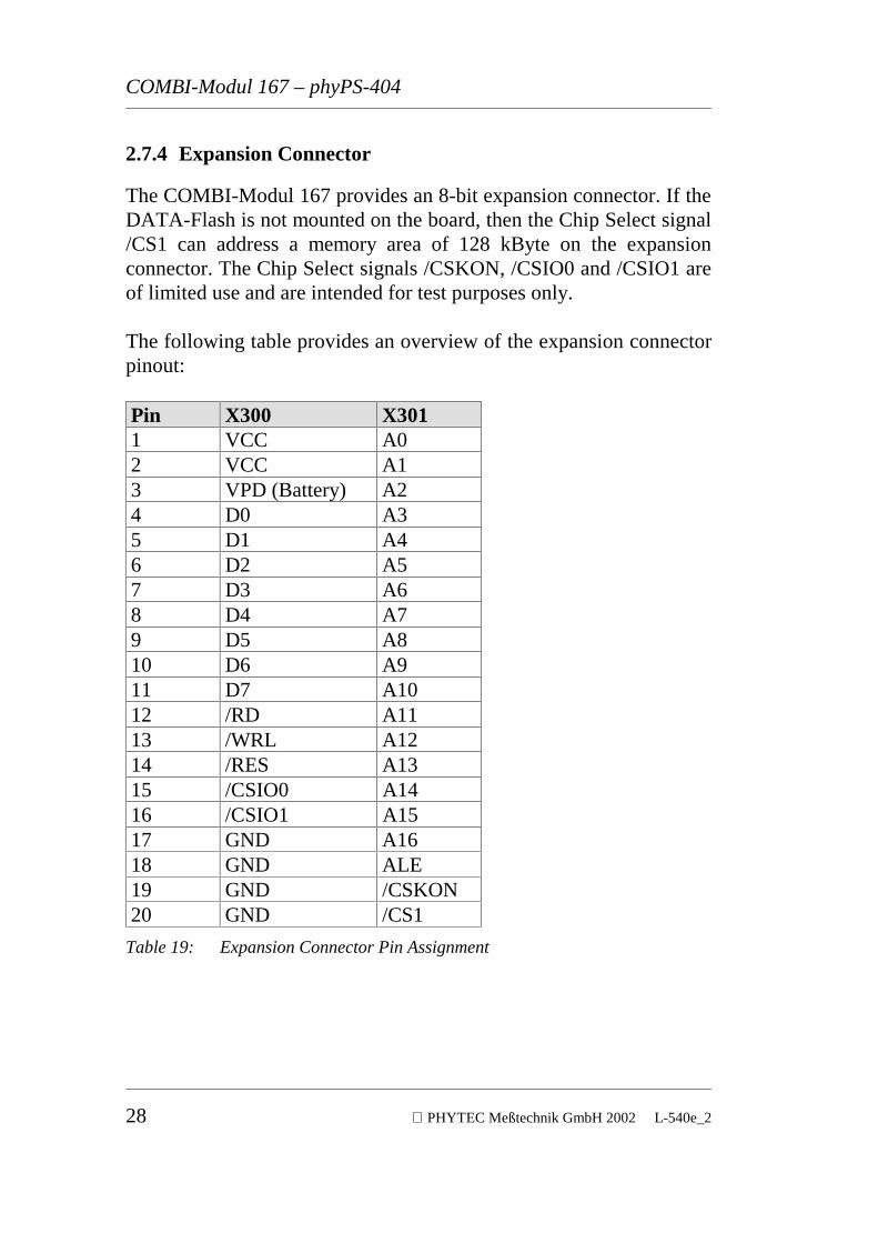
2.7.4 Expansion Connector
The COMBI-Modul 167 provides an 8-bit expansion connector. If theDATA-Flash is not mounted on the board, then the Chip Select signal/CS1 can address a memory area of 128 kByte on the expansionconnector. The Chip Select signals /CSKON, /CSIO0 and /CSIO1 areof limited use and are intended for test purposes only.
The following table provides an overview of the expansion connectorpinout:
Pin X300 X3011 VCC A02 VCC A13 VPD (Battery) A24 D0 A35 D1 A46 D2 A57 D3 A68 D4 A79 D5 A810 D6 A911 D7 A1012 /RD A1113 /WRL A1214 /RES A1315 /CSIO0 A1416 /CSIO1 A1517 GND A1618 GND ALE19 GND /CSKON20 GND /CS1
Table 19: Expansion Connector Pin Assignment

Components on the COMBI-Modul 167
PHYTEC Meßtechnik GmbH 2002 L-540e_2 29
2.8 Port Assignment Summary
The COMBICON connectors on the COMBI-Modul 167 display theindividual connector designator and the required polarity of thecorresponding input or output. The following tables show the pinassignment for the upper connector row (see Table 20) and the lowerconnector row (see Table 21). The assignment between input/outputsignal and the applicable internal signal level can be found in the"Description" column. The following conventions are used for thesignal states:
Inputs: Inputs are active LOW
Input voltage > 13 VDC: ‘0’ (TTL level) on port pinInput voltage < 5 VDC: ‘1’ (TTL level) on port pin
Outputs: Relay Outputs OUT0-7 are active HIGH
The relays are closed with a signal level of logical ‘1’ (TTL) on thecorresponding port pin.The relay contact is opened if a ‘0’ is written to the applicable outputpin.
Outputs: 24 V-Outputs OUT8-17 are active LOW
The output transistors have low resistance at a signal level ‘0’ (TTL)on the output of the port pin.The output transistors has high resistance if a ‘1’ is written to theapplicable output pin.
COMBI-Modul 167 – phyPS-404
30 PHYTEC Meßtechnik GmbH 2002 L-540e_2
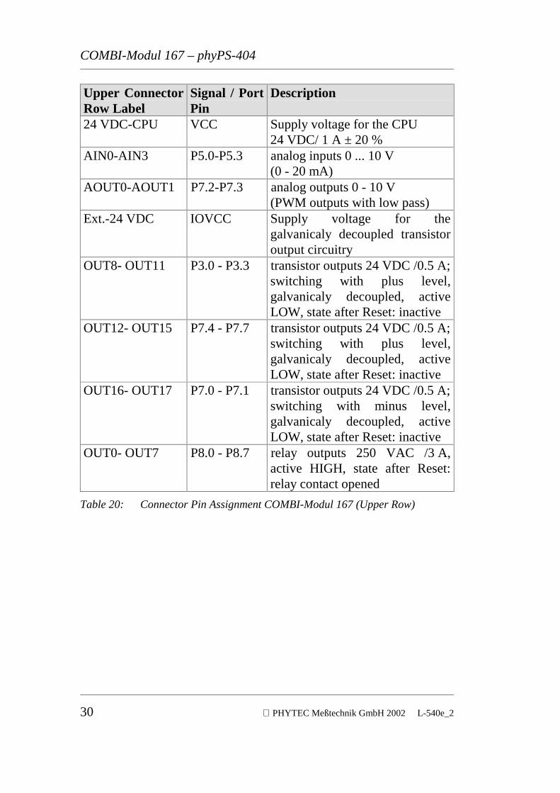
Upper ConnectorRow Label
Signal / PortPin
Description
24 VDC-CPU VCC Supply voltage for the CPU24 VDC/ 1 A ± 20 %
AIN0-AIN3 P5.0-P5.3 analog inputs 0 ... 10 V(0 - 20 mA)
AOUT0-AOUT1 P7.2-P7.3 analog outputs 0 - 10 V(PWM outputs with low pass)
Ext.-24 VDC IOVCC Supply voltage for thegalvanicaly decoupled transistoroutput circuitry
OUT8- OUT11 P3.0 - P3.3 transistor outputs 24 VDC /0.5 A;switching with plus level,galvanicaly decoupled, activeLOW, state after Reset: inactive
OUT12- OUT15 P7.4 - P7.7 transistor outputs 24 VDC /0.5 A;switching with plus level,galvanicaly decoupled, activeLOW, state after Reset: inactive
OUT16- OUT17 P7.0 - P7.1 transistor outputs 24 VDC /0.5 A;switching with minus level,galvanicaly decoupled, activeLOW, state after Reset: inactive
OUT0- OUT7 P8.0 - P8.7 relay outputs 250 VAC /3 A,active HIGH, state after Reset:relay contact opened
Table 20: Connector Pin Assignment COMBI-Modul 167 (Upper Row)

Components on the COMBI-Modul 167
PHYTEC Meßtechnik GmbH 2002 L-540e_2 31
Lower ConnectorRow Label
Signal /Port Pin
Description
RS-232 TxD RSTxD RS-232 signal level TxD outputof the C167CR internalasynchronous interface
RS-232 GND Ground Ground potential of theCOMBI-Modul 167 for RS-232connection at 3-pin clamp(Serial0)
RS-232 RxD RSRxD RS-232 signal level RxD input ofthe C167CR internalasynchronous interface
CAN HI CAN_H CAN_HIGH signal from the CANinterface, optically isolated
CAN LO CAN_L CAN_LOW signal from the CANinterface, optically isolated
CAN GND GROUND Ground potential of the CANinterface, optically isolated
IN0 - IN15 P2.0 - P2.15 24 VDC inputs, optically isolated,signals are inverted ( 24 VDCinput level results in a Low levelon the corresponding port pin),interrupt capable
IN16 - IN19 P5.4 - P5.7 24 VDC inputs, optically isolated,signals are inverted ( 24 VDCinput level results in a Low levelon the corresponding port pin)
IN20, IN21 P3.5, P3.6 24 VDC inputs, optically isolated,signals are inverted ( 24 VDCinput level results in a Low levelon the corresponding port pin)
IN22, IN23 P5.12, P5.13 24 VDC inputs, optically isolated,signals are inverted ( 24 VDCinput level results in a Low levelon the corresponding port pin)
Table 21: Connector Pin Assignment COMBI-Modul 167 (Lower Row)

COMBI-Modul 167 – phyPS-404
32 PHYTEC Meßtechnik GmbH 2002 L-540e_2
The following tables (see Table 22, Table 23 and Table 24) give anoverview of the pin assignments for additional peripheralcomponents, such as RTC, HEX-encoding switch, RUN/STOPswitch, Status LEDs and external UART.
Signal Port Pin DescriptionSCL P3.9 Clock line I2C busSDA P3.8 Data line I2C busIRTC P3.7 Temperature sensor and RTC interrupt lineCPUID.0 P5.11 HEX-encoding switch S301 bit 0, active HIGHCPUID.1 P5.10 HEX-encoding switch S301 bit 1, active HIGHCPUID.2 P5.9 HEX-encoding switch S301 bit 2, active HIGHCPUID.3 P5.8 HEX-encoding switch S301 bit 3, active HIGHCPUID.4 P3.15 HEX-encoding switch S301 bit 4, active HIGHCPUID.5 P3.13 HEX-encoding switch S301 bit 5, active HIGHCPUID.6 P5.15 HEX-encoding switch S301 bit 6, active HIGHCPUID.7 P5.14 HEX-encoding switch S301 bit 7, active HIGH
Table 22: Port Pin Assignment for I2C Bus, RTC Interrupt and HEX-EncodingSwitch
Signal Port Pin DescriptionRUN/ STOPswitch S303
RUN_SWP6.6
RUN/STOP switch for the COMBI-Modul 167 atRUN-SW1, input, active LOW
MRES, P3.4 RUN/STOP switch in position MRES,input, active LOW
RUN-LED D5, P4.4 RUN-LED (green), status indication,software programmable, output, active LOW
CANErr D6, P4.7 CAN-Error-LED (red), status indication,software programmable, output, active LOW
SYSErr D7, P6.5 SYSTEM error (red), status indication,software programmable, output, active LOW
PON D8 Power-on status indication (yellow)NUM U8, P6.7 Silicon serial number chip on port pin P6.7,
use of this chip depends on user softwareUART P6.3 /CS UART (U204, 2nd serial RS-232 interface)X10.1 TxD1 Transmit line second serial RS-232 interfaceX10.2 RxD1 Receive line second serial RS-232 interfaceX10.3 GND Ground
Table 23: Port Pin Assignment for RUN/STOP Switch, Status LEDs, S300 andSecond Serial Interface
Components on the COMBI-Modul 167
PHYTEC Meßtechnik GmbH 2002 L-540e_2 33
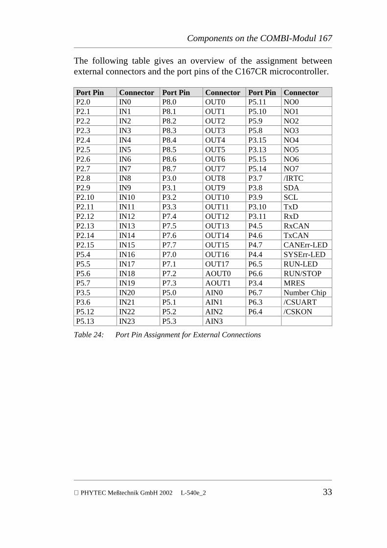
The following table gives an overview of the assignment betweenexternal connectors and the port pins of the C167CR microcontroller.
Port Pin Connector Port Pin Connector Port Pin ConnectorP2.0 IN0 P8.0 OUT0 P5.11 NO0P2.1 IN1 P8.1 OUT1 P5.10 NO1P2.2 IN2 P8.2 OUT2 P5.9 NO2P2.3 IN3 P8.3 OUT3 P5.8 NO3P2.4 IN4 P8.4 OUT4 P3.15 NO4P2.5 IN5 P8.5 OUT5 P3.13 NO5P2.6 IN6 P8.6 OUT6 P5.15 NO6P2.7 IN7 P8.7 OUT7 P5.14 NO7P2.8 IN8 P3.0 OUT8 P3.7 /IRTCP2.9 IN9 P3.1 OUT9 P3.8 SDAP2.10 IN10 P3.2 OUT10 P3.9 SCLP2.11 IN11 P3.3 OUT11 P3.10 TxDP2.12 IN12 P7.4 OUT12 P3.11 RxDP2.13 IN13 P7.5 OUT13 P4.5 RxCANP2.14 IN14 P7.6 OUT14 P4.6 TxCANP2.15 IN15 P7.7 OUT15 P4.7 CANErr-LEDP5.4 IN16 P7.0 OUT16 P4.4 SYSErr-LEDP5.5 IN17 P7.1 OUT17 P6.5 RUN-LEDP5.6 IN18 P7.2 AOUT0 P6.6 RUN/STOPP5.7 IN19 P7.3 AOUT1 P3.4 MRESP3.5 IN20 P5.0 AIN0 P6.7 Number ChipP3.6 IN21 P5.1 AIN1 P6.3 /CSUARTP5.12 IN22 P5.2 AIN2 P6.4 /CSKONP5.13 IN23 P5.3 AIN3
Table 24: Port Pin Assignment for External Connections

COMBI-Modul 167 – phyPS-404
34 PHYTEC Meßtechnik GmbH 2002 L-540e_2
Memory Models
PHYTEC Meßtechnik GmbH 2002 L-540e_2 35
3 Memory Models
3.1 Memory Configuration
3.1.1 Chip Select Signals
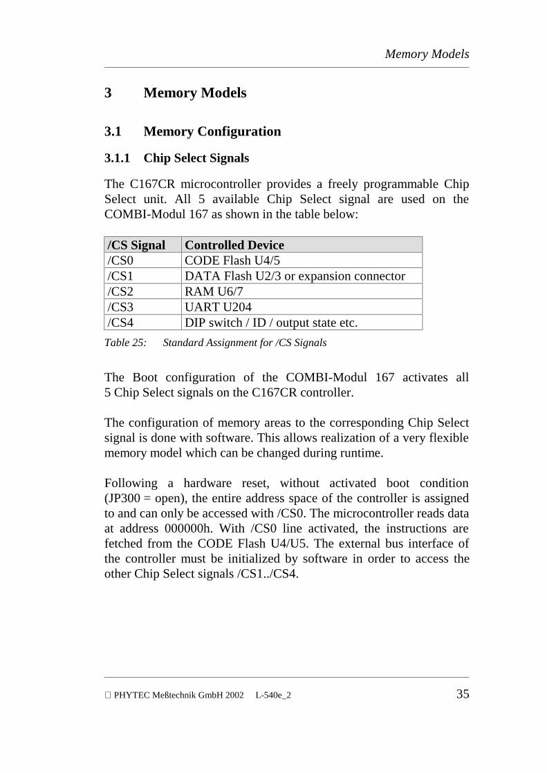
The C167CR microcontroller provides a freely programmable ChipSelect unit. All 5 available Chip Select signal are used on theCOMBI-Modul 167 as shown in the table below:
/CS Signal Controlled Device/CS0 CODE Flash U4/5/CS1 DATA Flash U2/3 or expansion connector/CS2 RAM U6/7/CS3 UART U204/CS4 DIP switch / ID / output state etc.
Table 25: Standard Assignment for /CS Signals
The Boot configuration of the COMBI-Modul 167 activates all5 Chip Select signals on the C167CR controller.
The configuration of memory areas to the corresponding Chip Selectsignal is done with software. This allows realization of a very flexiblememory model which can be changed during runtime.
Following a hardware reset, without activated boot condition(JP300 = open), the entire address space of the controller is assignedto and can only be accessed with /CS0. The microcontroller reads dataat address 000000h. With /CS0 line activated, the instructions arefetched from the CODE Flash U4/U5. The external bus interface ofthe controller must be initialized by software in order to access theother Chip Select signals /CS1../CS4.
COMBI-Modul 167 – phyPS-404
36 PHYTEC Meßtechnik GmbH 2002 L-540e_2
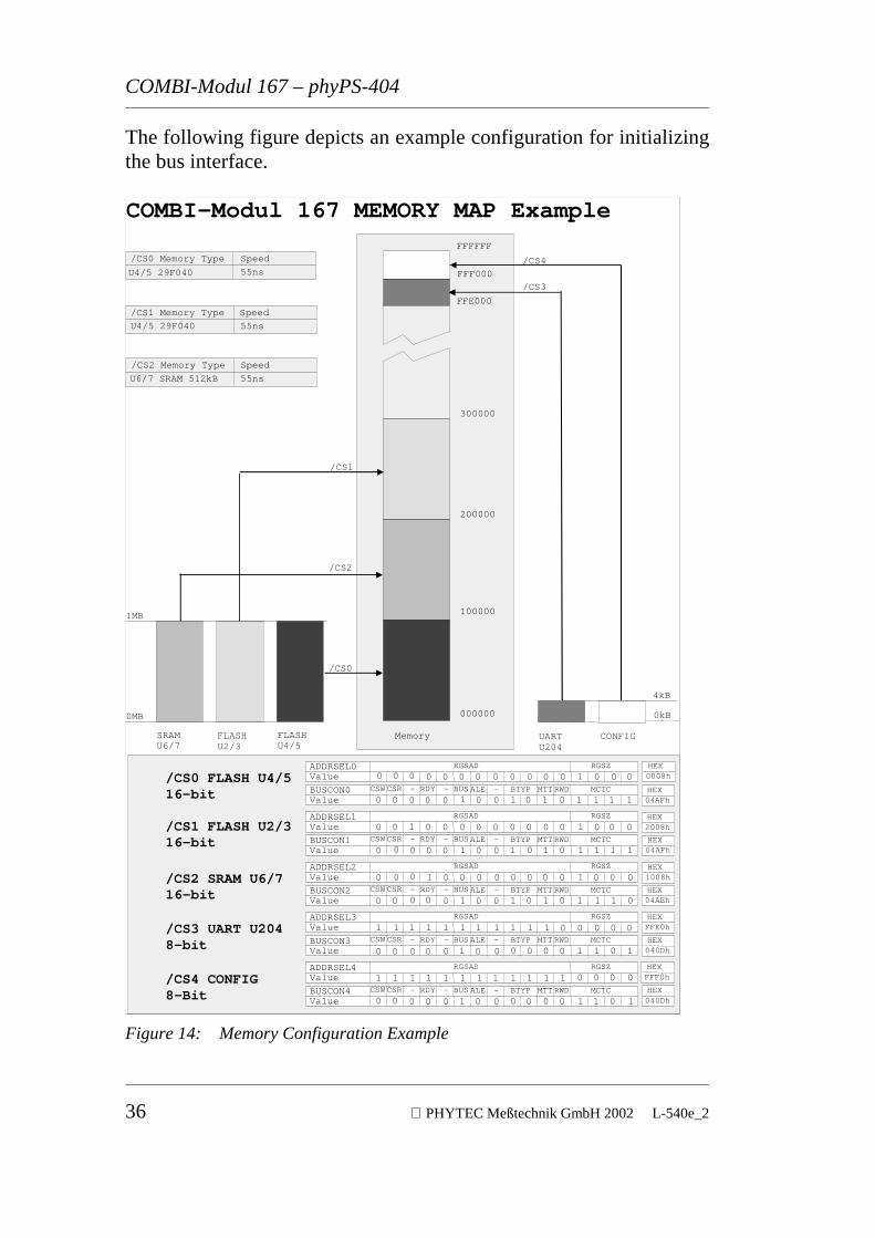
The following figure depicts an example configuration for initializingthe bus interface.
000000
100000
200000
300000
FFE000
FFFFFF
FFF000
COMBI-Modul 167 MEMORY MAP Example
/CS4
/CS3
/CS1
/CS2
/CS0
/CS0 FLASH U4/516-bit
/CS1 FLASH U2/316-bit
/CS2 SRAM U6/716-bit
/CS3 UART U2048-bit
/CS4 CONFIG8-Bit
Value
Value
ADDRSEL0
BUSCON0 CSW CSR - RDY - BUS ALE - BTYP MTTRWD MCTC
RGSAD RGSZ
Value
Value
ADDRSEL1
BUSCON1 CSW CSR - RDY - BUS ALE - BTYP MTTRWD MCTC
RGSAD RGSZ
Value
Value
ADDRSEL2
BUSCON2 CSW CSR - RDY - BUS ALE - BTYP MTTRWD MCTC
RGSAD RGSZ
Value
Value
ADDRSEL3
BUSCON3 CSW CSR - RDY - BUS ALE - BTYP MTTRWD MCTC
RGSAD RGSZ
Value
Value
ADDRSEL4
BUSCON4 CSW CSR - RDY - BUS ALE - BTYP MTTRWD MCTC
RGSAD RGSZ
Memory
0MB
1MB
0kB
4kB
SRAMU6/7
FLASHU2/3
FLASHU4/5
UARTU204
CONFIG
/CS0 Memory Type Speed
/CS1 Memory Type
/CS2 Memory Type
Speed
Speed
U4/5 29F040
U4/5 29F040
U6/7 SRAM 512kB
55ns
55ns
55ns
1
0 0 0 0 0 0 0 0 0 0 0 0
0 0 0 0 0 0 0 0 0 0 0
0 0 0 0 0 0 0 0 0 0 0
0
0 0 0
0 0 0
0 0 0
0 0 0 0
0 0 0 0
0
0
0
0
0
0
0
0
0
0
0
0
0
0
0
0 0
0 0
0 0
0 0
0 0
0
0
0
0
0
0
0
0
0
0
0
0
0
00
00
0
0
0
0
0 1
1
1
0 1
0 1
1 1 1
1
1 1
1
1 1 1
1
1 1 0
1 1
111
1
1 1 1
11 1
0
0
1
1
1 1 1 1 1 1 1 1 1 1 1
1 1 1 1 1 1 1 1 1 1 1 1
HEX0008h
HEX04AFh
HEX2008h
HEX04AFh
HEX1008h
HEX04AEh
HEXFFE0h
HEX040Dh
HEXFFF0h
HEX040Dh
Figure 14: Memory Configuration Example
Memory Models
PHYTEC Meßtechnik GmbH 2002 L-540e_2 37
In the BUSCONx register not only the bus type is configured, but alsothe timing parameters for the bus access.
By configuring the memory cycle wait state (Tc = 50 ns) and theread/write delay it is possible to use memory devices with accesstimes up to 100 ns at a bus cycle time of 150 ns. To run the controllerwithout wait state, memory devices with 55 ns access time must beinstalled. In this case, the bus cycle time is 100 ns. The read/writedelay should always be active (refer to the C167CR User’s Manualfor more information).
The following paragraph contains important information on timingcharacteristics. All information refers to a C167CR controller with a16-bit bus, demultiplexed, at 20 MHz CPU clock time (Fosz = 5 MHz).
Tc = 50 ns * wait state control (MCTC in BUSCON)Tf = 50 ns * tristate control (MTTC in BUSCON).
addresses stable until data valid: max. 70 ns + Tc SR1
/RD low until data valid: max. 55 ns + Tc SR1
/RD low until data valid (rd/wr delay): max. 30 ns + Tc SR1
/RD high until databus high-Z: max. 15 ns + Tf SR1
/RD high until data high-Z (rd/wr delay): max. 35 ns + Tf SR1
/CSx until data valid: max. 55 ns + Tc SR1
/RD and /WR low: min. 65 ns + Tc CC2
/RD and /WR low (rd/wr delay): min. 40 ns + Tc CC2
data valid until /WR high: min. 25 ns + Tc CC2
/WR high until data invalid: min. 15 ns + Tf CC2
The following sections contain example configurations of thecontroller for initializing the individual Chip Select signals.
1: SR = System Time (external circuitry must meet this timing criteria)2: CC = Controller Characteristic (the controller ensures this time for external
peripheral circuitry)
COMBI-Modul 167 – phyPS-404
38 PHYTEC Meßtechnik GmbH 2002 L-540e_2
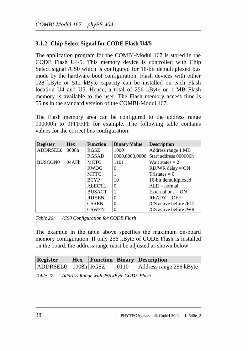
3.1.2 Chip Select Signal for CODE Flash U4/5
The application program for the COMBI-Modul 167 is stored in theCODE Flash U4/5. This memory device is controlled with ChipSelect signal /CS0 which is configured for 16-bit demultiplexed busmode by the hardware boot configuration. Flash devices with either128 kByte or 512 kByte capacity can be installed on each Flashlocation U4 and U5. Hence, a total of 256 kByte or 1 MB Flashmemory is available to the user. The Flash memory access time is55 ns in the standard version of the COMBI-Modul 167.
The Flash memory area can be configured to the address range000000h to 0FFFFFh for example. The following table containsvalues for the correct bus configuration:
Register Hex Function Binary Value DescriptionADDRSEL0 0008h RGSZ
RGSAD10000000.0000.0000
Address range 1 MBStart address 000000h
BUSCON0 04AFh MCTCRWDCMTTCBTYPALECTLBUSACTRDYENCSRENCSWEN
1101011001000
Wait states = 2RD/WR delay = ONTristates = 016-bit demultiplexedALE = normalExternal bus = ONREADY = OFF/CS active before /RD/CS active before /WR
Table 26: /CS0 Configuration for CODE Flash
The example in the table above specifies the maximum on-boardmemory configuration. If only 256 kByte of CODE Flash is installedon the board, the address range must be adjusted as shown below:
Register Hex Function Binary DescriptionADDRSEL0 0008h RGSZ 0110 Address range 256 kByte
Table 27: Address Range with 256 kByte CODE Flash
Memory Models
PHYTEC Meßtechnik GmbH 2002 L-540e_2 39
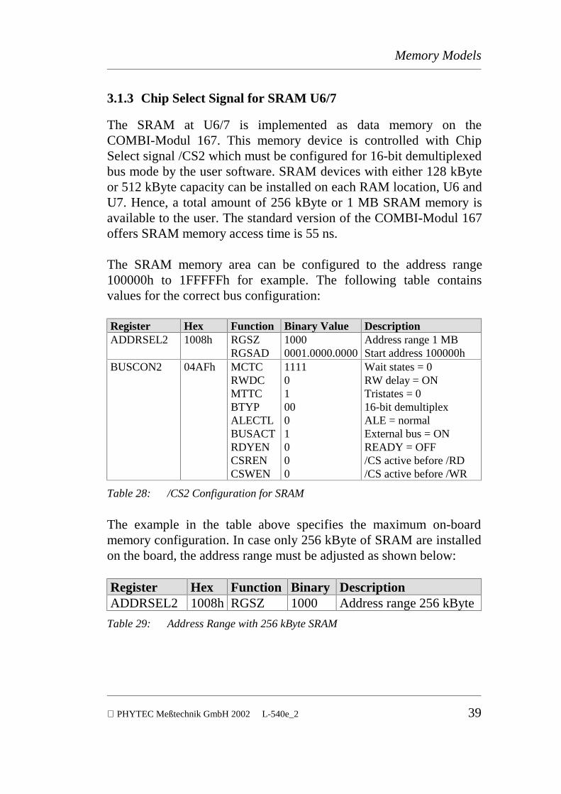
3.1.3 Chip Select Signal for SRAM U6/7
The SRAM at U6/7 is implemented as data memory on theCOMBI-Modul 167. This memory device is controlled with ChipSelect signal /CS2 which must be configured for 16-bit demultiplexedbus mode by the user software. SRAM devices with either 128 kByteor 512 kByte capacity can be installed on each RAM location, U6 andU7. Hence, a total amount of 256 kByte or 1 MB SRAM memory isavailable to the user. The standard version of the COMBI-Modul 167offers SRAM memory access time is 55 ns.
The SRAM memory area can be configured to the address range100000h to 1FFFFFh for example. The following table containsvalues for the correct bus configuration:
Register Hex Function Binary Value DescriptionADDRSEL2 1008h RGSZ
RGSAD10000001.0000.0000
Address range 1 MBStart address 100000h
BUSCON2 04AFh MCTCRWDCMTTCBTYPALECTLBUSACTRDYENCSRENCSWEN
1111010001000
Wait states = 0RW delay = ONTristates = 016-bit demultiplexALE = normalExternal bus = ONREADY = OFF/CS active before /RD/CS active before /WR
Table 28: /CS2 Configuration for SRAM
The example in the table above specifies the maximum on-boardmemory configuration. In case only 256 kByte of SRAM are installedon the board, the address range must be adjusted as shown below:
Register Hex Function Binary DescriptionADDRSEL2 1008h RGSZ 1000 Address range 256 kByte
Table 29: Address Range with 256 kByte SRAM

COMBI-Modul 167 – phyPS-404
40 PHYTEC Meßtechnik GmbH 2002 L-540e_2
3.1.4 Chip Select Signal for DATA Flash U2/3
The DATA Flash at U2/U3 is intended to serve as non-volatile datamemory on the COMBI-Modul 167. This memory device can bemounted on customer request. The Flash is controlled with ChipSelect signal /CS1 which must be configured for 16-bit demultiplexedbus mode by the user software.
Flash devices with either 128 kByte or 512 kByte capacity can beinstalled on each location, U2 and U3. Hence, a total of 256 kByte or1 MB DATA Flash memory is available to the user. The memoryaccess time is configured to 55 ns if the COMBI-Modul 167 ispopulated with the DATA Flash.The Flash memory area can be configured to the address range200000h to 2FFFFFh for example. The following table containsvalues for the correct bus configuration:
Register Hex Function Binary DescriptionADDRSEL1 2008h RGSZ
RGSAD10000010.0000.0000
Address range 1 MBStart address 100000h
BUSCON1 04AFh MCTCRWDCMTTCBTYPALECTLBUSACTRDYENCSRENCSWEN
1111011001000
Wait states = 0RD/WR delay = ONTristates = 016-bit demultiplexedALE = normalExternal bus = ONREADY = OFF/CS active before /RD/CS active before /WR
Table 30: /CS1 Configuration for DATA Flash
The example in the table above specifies the maximum on-boardmemory configuration. In case only 256 kByte of DATA Flash areinstalled on the board, the address range must be adjusted accordingto the size.
Alternatively, it is possible to use the /CS1 signal for control of theexpansion connector. In this case, the bus mode must be set to 8-bitdemultiplexed. The timing parameters depend on the componentsused at this expansion connector.
Memory Models
PHYTEC Meßtechnik GmbH 2002 L-540e_2 41
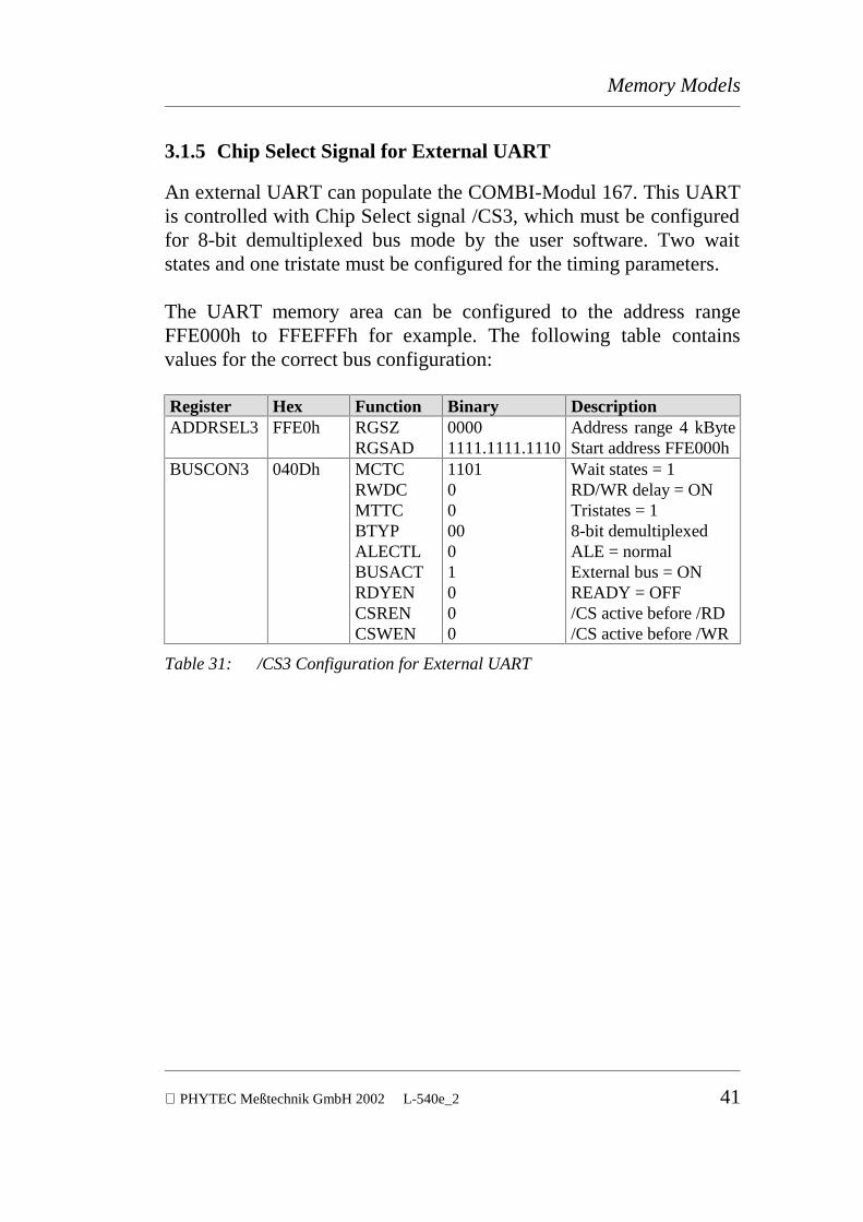
3.1.5 Chip Select Signal for External UART
An external UART can populate the COMBI-Modul 167. This UARTis controlled with Chip Select signal /CS3, which must be configuredfor 8-bit demultiplexed bus mode by the user software. Two waitstates and one tristate must be configured for the timing parameters.
The UART memory area can be configured to the address rangeFFE000h to FFEFFFh for example. The following table containsvalues for the correct bus configuration:
Register Hex Function Binary DescriptionADDRSEL3 FFE0h RGSZ
RGSAD00001111.1111.1110
Address range 4 kByteStart address FFE000h
BUSCON3 040Dh MCTCRWDCMTTCBTYPALECTLBUSACTRDYENCSRENCSWEN
1101000001000
Wait states = 1RD/WR delay = ONTristates = 18-bit demultiplexedALE = normalExternal bus = ONREADY = OFF/CS active before /RD/CS active before /WR
Table 31: /CS3 Configuration for External UART
COMBI-Modul 167 – phyPS-404
42 PHYTEC Meßtechnik GmbH 2002 L-540e_2
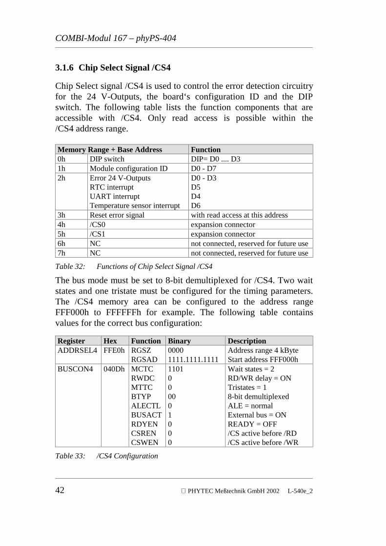
3.1.6 Chip Select Signal /CS4
Chip Select signal /CS4 is used to control the error detection circuitryfor the 24 V-Outputs, the board‘s configuration ID and the DIPswitch. The following table lists the function components that areaccessible with /CS4. Only read access is possible within the/CS4 address range.
Memory Range + Base Address Function0h DIP switch DIP= D0 .... D31h Module configuration ID D0 - D72h Error 24 V-Outputs
RTC interruptUART interruptTemperature sensor interrupt
D0 - D3D5D4D6
3h Reset error signal with read access at this address4h /CS0 expansion connector5h /CS1 expansion connector6h NC not connected, reserved for future use7h NC not connected, reserved for future use
Table 32: Functions of Chip Select Signal /CS4
The bus mode must be set to 8-bit demultiplexed for /CS4. Two waitstates and one tristate must be configured for the timing parameters.The /CS4 memory area can be configured to the address rangeFFF000h to FFFFFFh for example. The following table containsvalues for the correct bus configuration:
Register Hex Function Binary DescriptionADDRSEL4 FFE0h RGSZ
RGSAD00001111.1111.1111
Address range 4 kByteStart address FFF000h
BUSCON4 040Dh MCTCRWDCMTTCBTYPALECTLBUSACTRDYENCSRENCSWEN
1101000001000
Wait states = 2RD/WR delay = ONTristates = 18-bit demultiplexedALE = normalExternal bus = ONREADY = OFF/CS active before /RD/CS active before /WR
Table 33: /CS4 Configuration

Hints for Installing the COMBI-Modul 167
PHYTEC Meßtechnik GmbH 2002 L-540e_2 43
4 Hints for Installing the COMBI-Modul 167
Please note the following installation hints to ensure proper operationof the COMBI-Modul 167:
• The COMBI-Modul 167 design provides an EMC protectioncircuitry that is connected to protect earth (PE). Ensure that thecable that connects PE to the module is not longer than 100 mm.
• Take special care when installing cables for I/O connections.These cables should not be installed next to other cables that carryhigh power or signals with high noises. We recommend usingshielded cables when installing the product in high noiseenvironments in order to ensure proper EMC behavior.
• Ensure proper electrical separation of the low voltage for the 24 Vpower supply to the board.
• The COMBI-Modul 167 must be disconnected from a powersource while installing/deinstalling the unit.
• The COMBI-Modul 167 should be installed by trained personal(such as technicians) only.
• Shielded twisted pair cables are recommended for connecting theanalog inputs and outputs if the module is installed in high noiseenvironments.
• It is recommended to install cables for signal lines and controllines separate from cables that carry power and signals for motors.
• It is strongly recommended to avoid parallel installation of cableswith different electrical potentials.

COMBI-Modul 167 – phyPS-404
44 PHYTEC Meßtechnik GmbH 2002 L-540e_2
5 Hints for Operating the COMBI-Modul 167
• The COMBI-Modul 167 is not designed for use in life supportingsystems.
• We do not guarantee proper operation of the COMBI-Modul 167when used in high noise environments that exceed common EMCguidelines.
• All values for operation voltage and I/O signals on theCOMBI-Modul 167 may not exceed the specified maximum valuein order to avoid malfunction and destruction of the device.
• The COMBI-Modul 167 should not be used in a high humidityenvironment.
• The IP20 protection is guaranteed only if the clear plasticenclosure is installed and the COMBICON connectors areinserted.
Technical Specifications
PHYTEC Meßtechnik GmbH 2002 L-540e_2 45
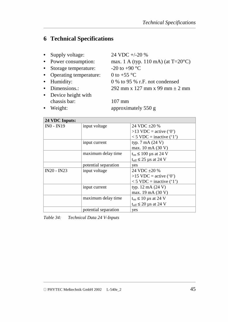
6 Technical Specifications
• Supply voltage: 24 VDC +/-20 %• Power consumption: max. 1 A (typ. 110 mA) (at T=20°C)• Storage temperature: -20 to +90 °C• Operating temperature: 0 to +55 °C• Humidity: 0 % to 95 % r.F. not condensed• Dimensions.: 292 mm x 127 mm x 99 mm ± 2 mm• Device height with
chassis bar: 107 mm• Weight: approximately 550 g
24 VDC Inputs:IN0 - IN19 input voltage 24 VDC ±20 %
>13 VDC = active (‘0’)< 5 VDC = inactive (‘1’)
input current typ. 7 mA (24 V)max. 10 mA (30 V)
maximum delay time ton ≤ 100 µs at 24 Vtoff ≤ 25 µs at 24 V
potential separation yesIN20 - IN23 input voltage 24 VDC ±20 %
>15 VDC = active (‘0’)< 5 VDC = inactive (‘1’)
input current typ. 12 mA (24 V)max. 19 mA (30 V)
maximum delay time ton ≤ 10 µs at 24 Vtoff ≤ 20 µs at 24 V
potential separation yes
Table 34: Technical Data 24 V-Inputs

COMBI-Modul 167 – phyPS-404
46 PHYTEC Meßtechnik GmbH 2002 L-540e_2
RelayOUT0-7 Relay maximum switching voltage 125 VAC/250 VAC
maximum switching current 3 A/2 Amaximum switching power 500 VAminimum switching power 200 mWresponse time typical 8 msfall time typical 12 msbounce time typical 1.5 mspotential separation relay contact winding 4 kVeff
relay contact to relay contact1 kVeff
expected life time 2*105 switching cycles
Table 35: Technical Data Relay Inputs
24 V-OutputsOUT8-15(transistor)
switched voltage pole consumer plus pole
switching voltage 24 VDC ±20 %output current 0.5 A / output; total current of
all outputs: max. 4 Amax. switching voltage 30 VDCmax. delay time ton ≤ 150 µs
toff ≤ 400 µserror detection yesshort circuit resistant yesovertemperature resistant yesprotection against overvoltage diode
OUT16-17(PWM)
switched voltage pole consumer minus pole
switching voltage 24 VDC ±20 %output current 0.5 A / output; total current of
all outputs: max. 1 Amax. switching voltage 30 VDCmax. delay time ton ≤ 15 µs at 24 V/ 0.5 A
toff ≤ 7,5 s at 24 V/ 0.5 Aprotection against overvoltage diode
supply voltagefor24 V-Outputs
input voltage 24 VDC/ ± 20 %,total currentof all outputs max.4 A, OUT8..OUT17
Table 36: Technical Data 24 V-Outputs
Technical Specifications
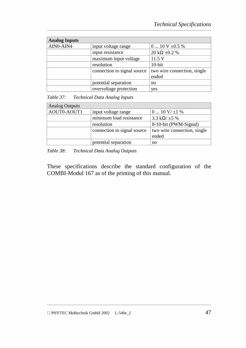
PHYTEC Meßtechnik GmbH 2002 L-540e_2 47
Analog InputsAIN0-AIN4 input voltage range 0 ... 10 V ±0.5 %
input resistance 20 kΩ ±0.2 %maximum input voltage 11.5 Vresolution 10-bitconnection to signal source two wire connection, single
endedpotential separation noovervoltage protection yes
Table 37: Technical Data Analog Inputs
Analog OutputsAOUT0-AOUT1 input voltage range 0 ... 10 V/ ±1 %
minimum load resistance 3.3 kΩ/ ±5 %resolution 8-10-bit (PWM-Signal)connection to signal source two wire connection, single
endedpotential separation no
Table 38: Technical Data Analog Outputs
These specifications describe the standard configuration of theCOMBI-Modul 167 as of the printing of this manual.

COMBI-Modul 167 – phyPS-404
48 PHYTEC Meßtechnik GmbH 2002 L-540e_2
Index
PHYTEC Meßtechnik GmbH 2002 L-540e_2 49
Index
/
/CS0...........................................38/CS1...........................................40/CS2...........................................39/CS3...........................................41
2
24 V-Outputs .............................1324 VDC-CPU ..............................924 VDC-Ext. ...............................924V Inputs IN0..IN23 ...............10
A
Analog Inputs ............................16Analog Outputs .........................17Assembler....................................7
B
Battery .......................................27Block Diagram ............................5
C
C 7CAN Bus Cable.........................21CAN Driver Library....................7CAN Interface ...........................21Changing the Battery.................27Chip Select Signal /CS4 ............42CODE Flash ..............................38COMBICON ...............................3COMBI-Modul............................3Compact Control System.............3Configuration for
CODE Flash..........................38Configuration for
DATA Flash..........................40Configuration for External
UART....................................41
Configuration for SRAM ..........39Connector Designator................29
D
DIP Switch ................................24Display and Control Units .........23
E
Expansion Connector ................28
F
Features .......................................4First RS-232 Interface ...............22FULL-CAN Interface ................21
H
HEX-Encoding Switch ........23, 32
I
I/O Port Arrangement of the 24V Inputs............................10
I2C Bus ......................................18I²C Bus.......................................18I²C EEPROM.............................19I²C EEPROM Address ..............19IGAS............................................3Index..........................................49Installation Hints .......................43Introduction .................................3
J
Jumper Configuration................26
L
Location of the Function Blocks .7
M
Memory Access Time....38, 39, 40Memory Configuration........26, 35

COMBI-Modul 167 – phyPS-404
50 PHYTEC Meßtechnik GmbH 2002 L-540e_2
N
Network Layer ............................ 7
O
Operating Hints......................... 44Overview..................................... 3
P
phyPS Driver............................... 7Port Assignment Summary ....... 29Power Supply .............................. 9PWM Outputs ........................... 15
R
Real-Time Clock....................... 18Relay Outputs............................ 12RESET ...................................... 26RTC........................................... 32RTC Address............................. 19RUN/STOP Switch ............. 25, 32
S
S300 .......................................... 24S301 .......................................... 23
S302...........................................23S303...........................................25SCL .....................................18, 19SDA.....................................18, 19Second RS-232 Interface ..........22Software Development Tools......7SRAM .......................................39Status LEDs.........................25, 32
T
Technical Specifications ...........45Temperature Sensor ..................20Temperature Sensor Address ....20Timing Characteristics ..............37
U
U2..............................................40U3..............................................40U4..............................................38U5..............................................38U6..............................................39U7..............................................39UART........................................32

Suggestions for Improvments
PHYTEC Meßtechnik GmbH 2002 L-540e_2
Document: COMBI-Modul 167Document number: L-540e_2, April 2002 How would you improve this manual?
Did you find any mistakes in this manual? page
Submitted by:Customer number:
Name:
Company:
Address:
Return to:PHYTEC Technologie Holding AGPostfach 100403D-55135 Mainz, GermanyFax : +49 (6131) 9221-33

Published by
PHYTEC Meßtechnik GmbH 2002 Ordering No. L-540e_2Printed in Germany