WHISKER FORMATION ON GALVANIC TIN …imim.pl/files/archiwum/Vol2B_2015/43.pdf · 1343 2.4....
5
A R C H I V E S O F M E T A L L U R G Y A N D M A T E R I A L S Volume 60 2015 Issue 2 DOI: 10.1515/amm-2015-0127 A.L. RADANYI * , A. SYCHEVA ** ,] , Z. GACSI * WHISKER FORMATION ON GALVANIC TIN SURFACE LAYER TWORZENIE WHISKERÓW NA POWIERZCHNIOWEJ WARSTWIE CYNY WYTWORZONEJ GALWANICZNIE The present work reports the effect of substrate composition, thickness of the tin electroplate and its morphology on pressure-induced tin whisker formation. Pure tin deposits of different thickness were obtained on a copper and brass substrates using methane sulfonic industrial bath. The deposits were compressed by a steel bearing ball forming imprint on the surface. The microstructure of tin whiskers obtained at the boundary of each imprint, their length and number were studied using both light and scanning electron microscopy. It was shown that the most intensive formation and growth of whiskers was observed in the first two hours. In general, brass substrate was shown to be more prone to whisker formation than copper independently of the tin coating thickness. The results have been compared with industrial bright tin finish on control unit socket leads and proposals have been made as to modification of the production process in order to minimize the risk of whiskering. Keywords: Tin whiskers, galvanic tin layer, mechanical stress, X-ray Fluorescence Spectrometry, Scanning Electron Mi- croscopy 1. Introduction The research of lead-free coatings and connections has been proceeding since 1946 to the present day [1-2]. It has been known for decades that on the surface of some low melt- ing metals including tin, cadmium and zinc, even at room temperature whisker formation is observed due to diffusion. At elevated temperatures whiskers can be formed on the alu- minum surface as well. The whiskers formed on the tin surface are single crystals of several micrometers in diameter and up to several millimeters long. Tin whiskers have excellent electrical conductivity, which is able to cause short circuit in small electrical devices. Earlier, this problem was solved by lead alloying (Arnold, 1956) [3], but nowadays the use of lead is prohibited by the RoHS Directive. There are many documented cases in which tin whiskers have resulted in the failure of electronic equipment: pacemaker failure (1986) in health-industry, F-15 radar failure (1986), auxiliary engine of a missile in the armaments industry, satellites were destroyed (Solidaridad 1) in space industry [4]. Whisker growth is influenced by many factors such as substrate material [5], residual stress in finish [6], grain size of finish [7] and so on. The most compelling theory for tin whisker growth is that it occurs due to a compressive stress [8]. Sources of stress in tin include plating residual stress, mechanical loading [9], scratches in the plating surface, plat- ing surface oxidation, intermetallic formation, and mismatches in the coefficient of thermal expansion between the plating and the underlying substrate [10-11]. It is already known that at elevated temperatures Cu-Sn intermetallic compounds are formed at the deposit-substrate interface, which causes addi- tional compressive stresses in the Sn layer, which are accord- ingly relieved by growth of Sn whiskers. In the case of connectors with pure tin or tin-based alloy coatings, pressure between the connector elements can produce pressure-induced tin whiskers. The nature of pressure-induced whiskers differs from that of spontaneous whiskers [12]. The former grow rapidly at room temperature, Cu-Sn intermetallic compound is not required for the growth. Mitigation practices such as increase of coating thickness, Ni, Ag barrier, reflow, heat treatment after plating yet cannot eliminate whiskers effectively to date [13-14], many questions remain. In this work a systematic study was conducted on re- lationship between mechanical compressive stress applied to the tin plating, substrate composition, Sn layer structure and thickness, and whisker formation intensity without formation of intermetallic compound. 2. Experimental 2.1. Tin electroplating procedure Substrate materials used in this study were pure copper and brass sheets with 70% Cu (Eurocircuits Ltd., Eger) and * INSTITUTE OF PHYSICAL METALLURGY, METAL FORMING AND NANOTECHNOLOGY, UNIVERSITY OF MISKOLC, MISKOLC, HUNGARY ** MTA-ME MATERIALS SCIENCE RESEARCH GROUP, HUNGARIAN ACADEMY OF SCIENCES, MISKOLC, HUNGARY ] Corresponding author: [email protected]
Transcript of WHISKER FORMATION ON GALVANIC TIN …imim.pl/files/archiwum/Vol2B_2015/43.pdf · 1343 2.4....
A R C H I V E S O F M E T A L L U R G Y A N D M A T E R I A L S
Volume 60 2015 Issue 2
DOI: 10.1515/amm-2015-0127
A.L. RADANYI∗, A. SYCHEVA∗∗ ,], Z. GACSI∗
WHISKER FORMATION ON GALVANIC TIN SURFACE LAYER
TWORZENIE WHISKERÓW NA POWIERZCHNIOWEJ WARSTWIE CYNY WYTWORZONEJ GALWANICZNIE
The present work reports the effect of substrate composition, thickness of the tin electroplate and its morphology onpressure-induced tin whisker formation. Pure tin deposits of different thickness were obtained on a copper and brass substratesusing methane sulfonic industrial bath. The deposits were compressed by a steel bearing ball forming imprint on the surface.The microstructure of tin whiskers obtained at the boundary of each imprint, their length and number were studied using bothlight and scanning electron microscopy. It was shown that the most intensive formation and growth of whiskers was observedin the first two hours. In general, brass substrate was shown to be more prone to whisker formation than copper independentlyof the tin coating thickness. The results have been compared with industrial bright tin finish on control unit socket leads andproposals have been made as to modification of the production process in order to minimize the risk of whiskering.
Keywords: Tin whiskers, galvanic tin layer, mechanical stress, X-ray Fluorescence Spectrometry, Scanning Electron Mi-croscopy
1. Introduction
The research of lead-free coatings and connections hasbeen proceeding since 1946 to the present day [1-2]. It hasbeen known for decades that on the surface of some low melt-ing metals including tin, cadmium and zinc, even at roomtemperature whisker formation is observed due to diffusion.At elevated temperatures whiskers can be formed on the alu-minum surface as well. The whiskers formed on the tin surfaceare single crystals of several micrometers in diameter andup to several millimeters long. Tin whiskers have excellentelectrical conductivity, which is able to cause short circuitin small electrical devices. Earlier, this problem was solvedby lead alloying (Arnold, 1956) [3], but nowadays the useof lead is prohibited by the RoHS Directive. There are manydocumented cases in which tin whiskers have resulted in thefailure of electronic equipment: pacemaker failure (1986) inhealth-industry, F-15 radar failure (1986), auxiliary engine ofa missile in the armaments industry, satellites were destroyed(Solidaridad 1) in space industry [4].
Whisker growth is influenced by many factors such assubstrate material [5], residual stress in finish [6], grain sizeof finish [7] and so on. The most compelling theory for tinwhisker growth is that it occurs due to a compressive stress[8]. Sources of stress in tin include plating residual stress,mechanical loading [9], scratches in the plating surface, plat-ing surface oxidation, intermetallic formation, and mismatches
in the coefficient of thermal expansion between the platingand the underlying substrate [10-11]. It is already known thatat elevated temperatures Cu-Sn intermetallic compounds areformed at the deposit-substrate interface, which causes addi-tional compressive stresses in the Sn layer, which are accord-ingly relieved by growth of Sn whiskers.
In the case of connectors with pure tin or tin-basedalloy coatings, pressure between the connector elementscan produce pressure-induced tin whiskers. The nature ofpressure-induced whiskers differs from that of spontaneouswhiskers [12]. The former grow rapidly at room temperature,Cu-Sn intermetallic compound is not required for the growth.Mitigation practices such as increase of coating thickness,Ni, Ag barrier, reflow, heat treatment after plating yet cannoteliminate whiskers effectively to date [13-14], many questionsremain. In this work a systematic study was conducted on re-lationship between mechanical compressive stress applied tothe tin plating, substrate composition, Sn layer structure andthickness, and whisker formation intensity without formationof intermetallic compound.
2. Experimental
2.1. Tin electroplating procedure
Substrate materials used in this study were pure copperand brass sheets with 70% Cu (Eurocircuits Ltd., Eger) and
∗ INSTITUTE OF PHYSICAL METALLURGY, METAL FORMING AND NANOTECHNOLOGY, UNIVERSITY OF MISKOLC, MISKOLC, HUNGARY∗∗ MTA-ME MATERIALS SCIENCE RESEARCH GROUP, HUNGARIAN ACADEMY OF SCIENCES, MISKOLC, HUNGARY] Corresponding author: [email protected]
1342
size of 100×80×1 mm. As a preparation, after rinsing withdistilled water the samples were degreased in acetone solu-tion at 30◦C for 25 min on an ultrasonic bath. After thatetching with 2% HNO3 solution was performed for 1 minin order to remove any oxide from the surface. These sheetswere electroplated using a commercial aqueous electroplatingbath Restin BMAT PC of the following composition: Sn (II)20 g/l, methane sulfonic acid 200 g/l, primary (10 vol.%) andsecondary (0.6 vol.%) additives. The main function of theadditives is providing fine grain structure and smooth densedeposit. Another purpose of the additives is to protect the dis-solved Sn2+ ions from oxidation to Sn4+ during electroplating.The electroplating was performed for 3 and 10 minutes and acurrent intensity of 1 A in a specially shaped container “Hullcell” having the cathode at a pre-defined angle to the anode(Fig. 1). It allowed producing a range of current densities andtin deposit thicknesses.
Fig. 1. Schematic presentation of the Hull cell (solution volume used– 267 ml) placed in a water bath for temperature control
The anode was a pure tin sheet, and the cathode platewas a pure copper or brass sheet both immersed vertically inthe electrolyte solution. The current densities produced in theHull cell can be calculated based on the geometrical data ofthe cell via Eq. 1:
−i = I(5.1 − 5.24 · lgX) (1)
where i – current density (A/dm2), I – total current intensity(A), X – distance from the high-current-density end of thepanel. Thus, the calculated current density along the sheetvaried in the range 0.1-5 A/dm2.
2.2. Estimation of tin deposit thickness
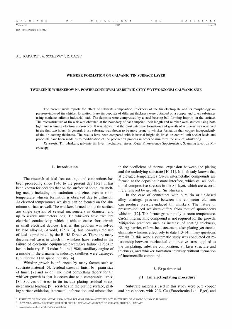
The freshly deposited tin layers were examined by HelmutFisher GmbH + Co. KG X-ray Fluorescence (XRF) Spectrom-eter at 50 kV in order to estimate tin layer thickness [15]. TheX-ray fluorescence spectra were collected by a silicon PINdetector of high-energy resolution (<200 eV). Samples weremeasured for 60 s using the utmost collimator (0.6 mm di-ameter). WinFTM (Windows-based) v.6.20 software has beenused including fundamental parameter method for computa-tion. The XRF results on relationship between current densityproduced during tin electrodeposition and tin deposit thicknesson the copper or brass substrates are presented in Fig. 2.
Fig. 2. Dependencies of tin deposit thickness on the current densityafter 3 and 10 minutes of electrodeposition
2.3. Pressure-induced tin whisker formation
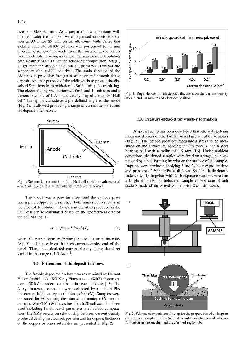
A special setup has been developed that allowed studyingmechanical stress on the formation and growth of tin whiskers(Fig. 3). The device produces mechanical stress to be mea-sured on the surface by loading it with force F via a steelbearing ball with a radius of 1.5 mm [16]. Under ambientconditions, the tinned samples were fixed on a stage and com-pressed by a ball forming imprint on the surface of the sample.Imprints were produced applying 2 and 24 hour exposure timeand pressure of 3000 MPa at different Sn deposit thickness.Independently, imprints with 24 h exposure were prepared ona bright tin finish of industrial sample (motor control unitsockets made of tin coated copper with 2 µm tin layer).
Fig. 3. Scheme of experimental setup for the preparation of an imprinton a tinned sample surface (a) and possible mechanism of whiskerformation in the mechanically deformed region (b)
1343
2.4. Estimation of length and number of whiskers
The microstructure of tin whiskers obtained, their lengthand number at the boundary of each imprint were studied usingZeiss EVO MA and Axio Imager Correlative Light ElectronMicroscopy system. First, the coordinates of imprints weresaved by the optical microscope software. In the second step,the sample stage together with the sample were placed in thescanning electron microscope (SEM), and the imprints werefound automatically by using the previously identified coordi-nates. After that the whiskers formed at the interface betweendeformed and non-deformed surfaces were observed by SEM.
3. Results and discussion
3.1. Effect of mechanical stress and its exposure time onwhisker formation
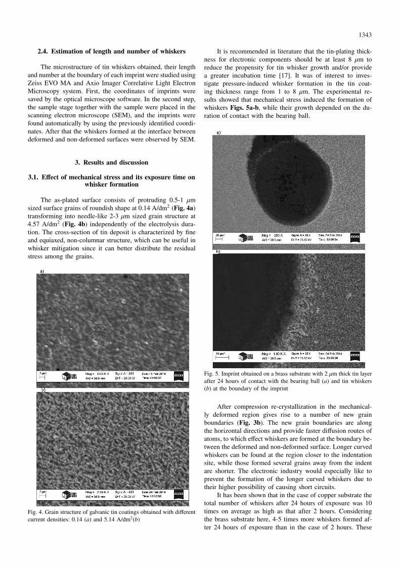
The as-plated surface consists of protruding 0.5-1 µmsized surface grains of roundish shape at 0.14 A/dm2 (Fig. 4a)transforming into needle-like 2-3 µm sized grain structure at4.57 A/dm2 (Fig. 4b) independently of the electrolysis dura-tion. The cross-section of tin deposit is characterized by fineand equiaxed, non-columnar structure, which can be useful inwhisker mitigation since it can better distribute the residualstress among the grains.
Fig. 4. Grain structure of galvanic tin coatings obtained with differentcurrent densities: 0.14 (a) and 5.14 A/dm2(b)
It is recommended in literature that the tin-plating thick-ness for electronic components should be at least 8 µm toreduce the propensity for tin whisker growth and/or providea greater incubation time [17]. It was of interest to inves-tigate pressure-induced whisker formation in the tin coat-ing thickness range from 1 to 8 µm. The experimental re-sults showed that mechanical stress induced the formation ofwhiskers Figs. 5a-b, while their growth depended on the du-ration of contact with the bearing ball.
Fig. 5. Imprint obtained on a brass substrate with 2 µm thick tin layerafter 24 hours of contact with the bearing ball (a) and tin whiskers(b) at the boundary of the imprint
After compression re-crystallization in the mechanical-ly deformed region gives rise to a number of new grainboundaries (Fig. 3b). The new grain boundaries are alongthe horizontal directions and provide faster diffusion routes ofatoms, to which effect whiskers are formed at the boundary be-tween the deformed and non-deformed surface. Longer curvedwhiskers can be found at the region closer to the indentationsite, while those formed several grains away from the indentare shorter. The electronic industry would especially like toprevent the formation of the longer curved whiskers due totheir higher possibility of causing short circuits.
It has been shown that in the case of copper substrate thetotal number of whiskers after 24 hours of exposure was 10times on average as high as that after 2 hours. Consideringthe brass substrate here, 4-5 times more whiskers formed af-ter 24 hours of exposure than in the case of 2 hours. These
1344
data confirm that the most intensive formation and growth ofwhiskers is observed in the first hours of contact with thebearing ball. The length of whiskers formed on the imprintswas also measured. Generally, it can be stated that the longerwas the exposure time, the greater was the average length ofthe whiskers formed. In the case of 2 hour exposure time theaverage length was 1 micrometer, while in the case of 24 hoursit was 7 micrometers. Above this exposure time no significantgrowth was observed.
3.2. Effect of tin deposit thickness and substratecomposition on whisker formation
It is also believed [5] that the presence of Zn in thebrass substrates suppresses the formation of Cu-Sn intermetal-lic compounds, thereby reducing the risk of growth of longwhiskers. In current experiments the intermetallic layer wasundetectable (according to SEM cross-sectional analysis) be-cause the deposit was obtained at room temperature. Fig. 6features dependencies of the average whisker length on tindeposit thickness after 24 hours of contact with the bearingball for both copper and brass substrates.
Fig. 6. Average whisker length vs. tin deposit thickness after 24 hoursof contact with the bearing ball
In general, brass was shown to be more prone to whiskerformation than copper. This observation can be explained byhigher hardness of brass, which does not neutralize but ratherinduces additional mechanical stress in the tin plating. It canbe seen that in the case of brass substrates after 24 hours ofexposure the whiskers are similar in average length but thehighest values were observed in the range of 4-5 µm thicktin layer. The longest whiskers on the copper substrate wereobserved in the case of 3 µm thick tin layer.
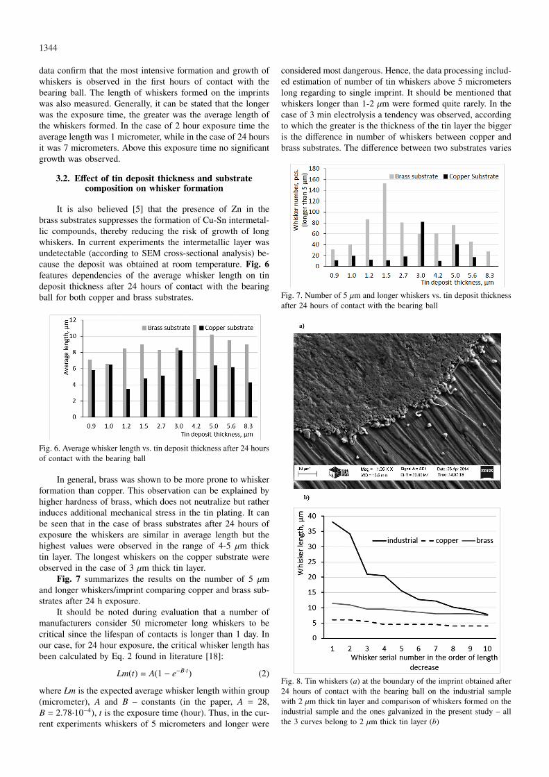
Fig. 7 summarizes the results on the number of 5 µmand longer whiskers/imprint comparing copper and brass sub-strates after 24 h exposure.
It should be noted during evaluation that a number ofmanufacturers consider 50 micrometer long whiskers to becritical since the lifespan of contacts is longer than 1 day. Inour case, for 24 hour exposure, the critical whisker length hasbeen calculated by Eq. 2 found in literature [18]:
Lm(t) = A(1 − e−B·t) (2)
where Lm is the expected average whisker length within group(micrometer), A and B – constants (in the paper, A = 28,B = 2.78·10−4), t is the exposure time (hour). Thus, in the cur-rent experiments whiskers of 5 micrometers and longer were
considered most dangerous. Hence, the data processing includ-ed estimation of number of tin whiskers above 5 micrometerslong regarding to single imprint. It should be mentioned thatwhiskers longer than 1-2 µm were formed quite rarely. In thecase of 3 min electrolysis a tendency was observed, accordingto which the greater is the thickness of the tin layer the biggeris the difference in number of whiskers between copper andbrass substrates. The difference between two substrates varies
Fig. 7. Number of 5 µm and longer whiskers vs. tin deposit thicknessafter 24 hours of contact with the bearing ball
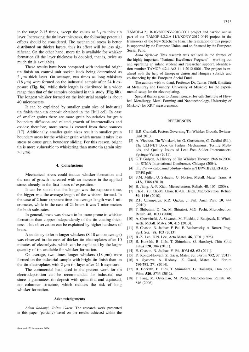
Fig. 8. Tin whiskers (a) at the boundary of the imprint obtained after24 hours of contact with the bearing ball on the industrial samplewith 2 µm thick tin layer and comparison of whiskers formed on theindustrial sample and the ones galvanized in the present study – allthe 3 curves belong to 2 µm thick tin layer (b)
1345
in the range 2-15 times, except the values at 3 µm thick tinlayer. Increasing the tin layer thickness, the following potentialeffects should be considered. The mechanical stress is betterdistributed on thicker layers, thus its effect will be less sig-nificant. On the other hand, more tin is available for whiskerformation (if the layer thickness is doubled, that is, twice asmuch tin is available).
These results have been compared with industrial brighttin finish on control unit socket leads being determined as2 µm thick layer. On average, two times as long whiskers(18 µm) were formed on the industrial sample after 24 h ex-posure (Fig. 8a), while their length is distributed in a widerrange than that of the samples obtained in this study (Fig. 8b).The longest whisker formed on the industrial sample is about40 micrometers.
It can be explained by smaller grain size of industrialtin finish than tin deposit obtained in the Hull cell. In caseof smaller grains there are more grain boundaries for grainboundary diffusion and related growth of intermetallics andoxides; therefore, more stress is created from these sources[17]. Additionally, smaller grain sizes result in smaller grainboundary areas for the whisker grain which means it takes lessstress to cause grain boundary sliding. For this reason, brighttin is more vulnerable to whiskering than matte tin (grain size>1 µm).
4. Conclusions
Mechanical stress could induce whisker formation andthe rate of growth increased with an increase in the appliedstress already in the first hours of exposition.
It can be stated that the longer was the exposure time,the bigger was the average length of the whiskers formed. Inthe case of 2 hour exposure time the average length was 1 mi-crometer, while in the case of 24 hours it was 7 micrometersfor both substrates.
In general, brass was shown to be more prone to whiskerformation than copper independently of the tin coating thick-ness. This observation can be explained by higher hardness ofbrass.
A tendency to form longer whiskers (8-10 µm on average)was observed in the case of thicker tin electroplates after 10minutes of electrolysis, which can be explained by the largerquantity of tin available for whisker formation.
On average, two times longer whiskers (18 µm) wereformed on the industrial sample with bright tin finish than onthe tin electroplates with 2 µm tin layer after 24 h exposure.
The commercial bath used in the present work for tinelectrodeposition can be recommended for industrial usesince it guarantees tin deposit with quite fine and equiaxed,non-columnar structure, which reduces the risk of longwhisker formation.
Acknowledgements
Adam Radanyi, Zoltan Gacsi: The research work presentedin this paper (partially) based on the results achieved within the
TAMOP-4.2.1.B-10/2/KONV-2010-0001 project and carried out aspart of the TAMOP-4.2.2.A-11/1/KONV-2012-0019 project in theframework of the New Szechenyi Plan. The realization of this projectis supported by the European Union, and co-financed by the EuropeanSocial Fund.
Anna Sycheva: This research was realized in the frames ofthe highly important “National Excellence Program” – working outand operating an inland student and researcher support, identifica-tion number TAMOP 4.2.4.A/2-11-1-2012-0001. The project is re-alized with the help of European Union and Hungary subsidy andco-financing by the European Social Fund.
The authors wish to thank Professor Dr. Tamas Torok (Instituteof Metallurgy and Foundry, University of Miskolc) for the experi-mental setup for tin electroplating.
Special thanks goes to Daniel Koncz-Horvath (Institute of Phys-ical Metallurgy, Metal Forming and Nanotechnology, University ofMiskolc) for XRF measurements.
REFERENCES
[1] E.R. Crandall, Factors Governing Tin Whisker Growth, Switzer-land 2013.
[2] A. Vicenzo, Tin Whiskers, in: G. Grossmann, C. Zardini (Ed.),The ELFNET Book on Failure Mechanisms, Testing Meth-ods, and Quality Issues of Lead-Free Solder Interconnects,Springer-Verlag (2011).
[3] G.T. Galyon, A History of Tin Whisker Theory: 1946 to 2004,in: STMA International Conference, Chicago (2004).
[4] http://www.calce.umd.edu/tin-whiskers/TINWHISKERFAIL-URES.pdf.
[5] S.M. Miller, U. Sahaym, G. Norton, Metall. Mater. Trans. A41A, 3386 (2010).
[6] B. Jiang, A.-P. Xian, Microelectron. Reliab. 48, 105. (2008).[7] Ch.-F. Yu, Ch.-M. Chan, K.-Ch. Hsieh, Microelectron. Reliab.
50, 1146 (2010).[8] R.F. Champaign, R.R. Ogden, J. Fail. Anal. Prev. 10, 444
(2010).[9] T. Shibutani, Q. Yu, M. Shiratori, M.G. Pecht, Microelectron.
Reliab. 48, 1033 (2008).[10] A. Czerwinski, A. Skwarek, M. Plushka, J. Ratajczak, K. Witek,
Arch. Metall. Mater. 58, 415 (2013).[11] E. Chason, N. Jadhav, F. Pei, E. Buchovecky, A. Bower, Prog.
Surf. Sci. 88, 103 (2013).[12] B.-Z. Lee, D.N. Lee, Acta Mater. 46, 3701 (1998).[13] B. Horvath, B. Illes, T. Shinohara, G. Harsanyi, Thin Solid
Films 520, 384 (2011).[14] E. Chason, N. Jadhav, F. Pei, JOM 63, 62 (2011).[15] D. Koncz-Horvath, Z. Gacsi, Mater. Sci. Forum 752, 37 (2013).[16] A. Sycheva, A. Radanyi, Z. Gacsi, Mater. Sci. Forum
790-791, 271 (2014).[17] B. Horvath, B. Illes, T. Shinohara, G. Harsanyi, Thin Solid
Films 520, 5733 (2012).[18] T. Fang, M. Osterman, M. Pecht, Microelectron. Reliab. 46,
846 (2006).
Received: 20 November 2014.