Gates – Part 1
38
04 GATES1 Page 1 Sistem Komputer NAROTAMA Gates – Part 1
-
Upload
bethany-cote -
Category
Documents
-
view
32 -
download
0
description
Gates – Part 1. drain. drain. drain. no current flows. gate. 3 volts. 0 volts. current flows. source. source. source. Gates are Built With Transistors. nFet. nFetOn. nFetOff. N-type field-effect transistor = nFet. source. source. source. no current flows. gate. 0 volts. - PowerPoint PPT Presentation
Transcript of Gates – Part 1

04 GATES1 Page 1
Sistem Komputer NAROTAMA
Gates – Part 1

04 GATES1 Page 2
Sistem Komputer NAROTAMA
Gates are Built With Transistors
nFet
gate
drain
source
3 volts
drain
source
0 volts
drain
source
currentflows
nocurrentflows
nFetOn nFetOff
N-type field-effect transistor = nFet

04 GATES1 Page 3
Sistem Komputer NAROTAMA
Gates are Built With Transistors
pFet pFetOn pFetOff
gate
source
drain
0 volts 3 voltscurrentflows
nocurrentflows
source
drain
source
drain
P-type field-effect transistor = pFet

04 GATES1 Page 4
Sistem Komputer NAROTAMA
Complement
Also known as invert or not.
x x'0 11 0
x’x
This is a schematic symbol.It is a graphical representationof a circuit which implementsthe operation.

04 GATES1 Page 5
Sistem Komputer NAROTAMA
FET-Based Inverter
Vin Vout
Vcc=3V
GND=0V
3V0V
0V 3V
off
on
on
off
Vcc=3V
GND=0V
Vcc=3V
GND=0V

04 GATES1 Page 6
Sistem Komputer NAROTAMA
AND and OR Gates
A B Q=A•B
0 0 00 1 01 0 01 1 1
A
BQ
A
BQ
A B Q=A+B
0 0 00 1 11 0 11 1 1

04 GATES1 Page 7
Sistem Komputer NAROTAMA
Boolean Expressions and GatesEach Boolean expression has a corresponding realization with logic gates.
A’
BC
F
F = A’ + B C

04 GATES1 Page 8
Sistem Komputer NAROTAMA
NAND Gates
A
BQ
A B Q=(A•B)'
0 0 10 1 11 0 11 1 0
NAND
A
BQ
A
BQ
Q is true iff A AND B are true
Q is false iff A AND B are true
AND
NAND

04 GATES1 Page 9
Sistem Komputer NAROTAMA
FET-Based NAND Gate
A
B
BA
Vcc
GND
F
Vcc
GND
1
1
11 off
on
off
on
0
Vcc
GND
1
0
01 off
on
on
off
1
04 GATES1 Page 10
Sistem Komputer NAROTAMA
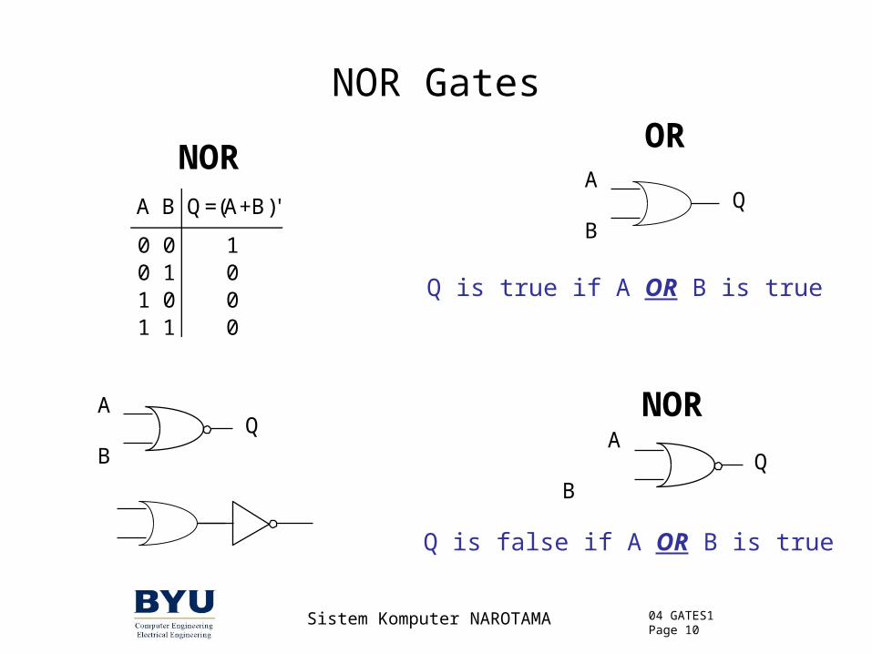
NOR Gates
A B Q=(A+B)'
0 0 10 1 01 0 01 1 0
A
BQ
NOR
A
BQ
A
BQ
Q is true if A OR B is true
Q is false if A OR B is true
OR
NOR

04 GATES1 Page 11
Sistem Komputer NAROTAMA
FET-Based NOR Gate
A
B
BA
F
Can you complete the truth table?
A B F
0v 0v ?0v 5v ?5v 0v ?5v 5v ?

04 GATES1 Page 12
Sistem Komputer NAROTAMA
FET-Based Gates
• P-type FETs must be on top of gate• N-type FETs must be on bottom of gate
– Due to electrical characteristics of the two FET types
• Output is driven to either ‘1’ or ‘0’– never both– never neither

04 GATES1 Page 13
ECEn/CS 224
Exclusive-OR (XOR)
Output is true iff inputs are different.
A
B
Q = A B = A’B + AB’
Another definition: C is true if A /= B
A B Q = A B
0 0 00 1 11 0 11 1 0
04 GATES1 Page 14
Sistem Komputer NAROTAMA
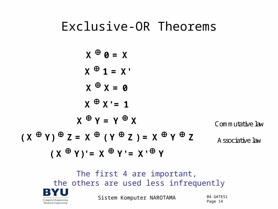
Exclusive-OR Theorems
X 0 = X
X 1 = X'
X X = 0
X X' = 1
X Y = Y X Commutative law
( X Y) Z = X ( Y Z ) = X Y Z Associative law
( X Y)' = X Y' = X' Y
The first 4 are important,
the others are used less infrequently

04 GATES1 Page 15
Sistem Komputer NAROTAMA
Equivalence Operation
denotes equivalence (also written as X==Y)
Output is true iff inputs are equal
X
Y
Q = (X==Y)= X’Y’ + XY
X Y X==Y
0 0 10 1 01 0 01 1 1
04 GATES1 Page 16
Sistem Komputer NAROTAMA
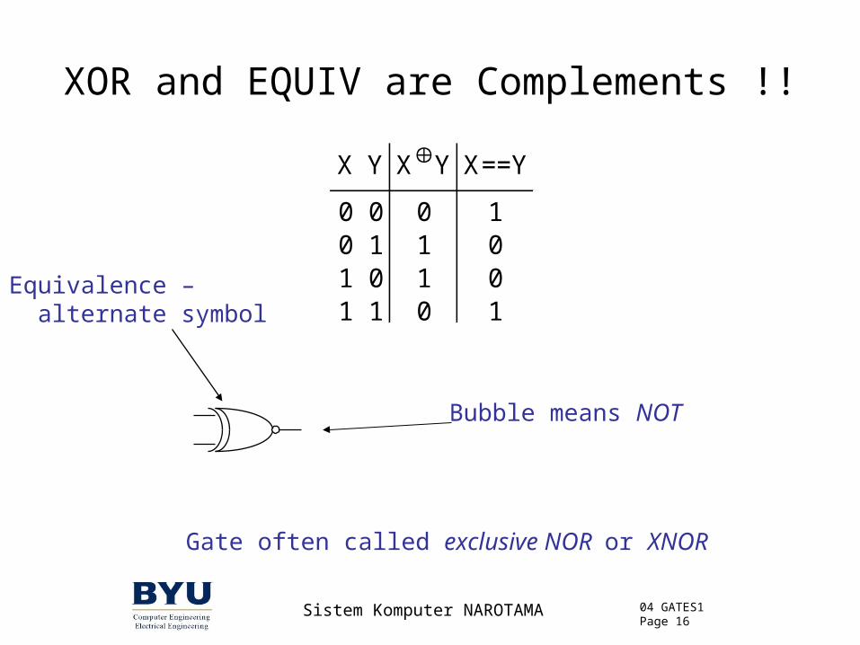
XOR and EQUIV are Complements !!
X Y XY X==Y
0 0 0 10 1 1 01 0 1 01 1 0 1
Gate often called exclusive NOR or XNOR
Bubble means NOT
Equivalence – alternate symbol

04 GATES1 Page 17
Sistem Komputer NAROTAMA
Multi-Input Gates
A
B
BA
Vcc
GND
F
C
C
A
B
BA
Vcc
GND
F
Which one will be slower/faster?

04 GATES1 Page 18
Sistem Komputer NAROTAMA
Alternative Gate Symbols
The symbolic meaning of the circuit should be clear from what
you draw…

04 GATES1 Page 19
Sistem Komputer NAROTAMA
Alternative Gate Symbols
Q is true if A is false OR B is false
A
BQ
Q is true iff A is false AND B is false
A B Q
0 0 10 1 11 0 11 1 0
A B Q
0 0 10 1 01 0 01 1 0
A
BQ A
BQ
A
BQ

04 GATES1 Page 20
Sistem Komputer NAROTAMA
Alternative Gate Symbols
Turn on sprinklers if it is not a holiday and it is not a weekend
or?
The problem statement uses AND, so use the AND symbol

04 GATES1 Page 21
Sistem Komputer NAROTAMA
Alternative Gate Symbols
Turn off the sprinklers if it is a holiday or it is a weekend
or?
The problem statement uses OR, so use the OR symbol

04 GATES1 Page 22
Sistem Komputer NAROTAMA
Another Example
• Design a circuit to determine whether the bits of a 4-bit wire are all zero
This is the appropriate symbol to use…

04 GATES1 Page 23
Sistem Komputer NAROTAMA
Mixed Symbols
• Such a gate doesn’t likely exist• Build from AND gate and inverter• Simplifies schematics
– enhanced readability
Q is true iff A is false AND B is true
A
BQ

04 GATES1 Page 24
Sistem Komputer NAROTAMA
Single Gate Conversion Rules
• Change symbol– AND to OR– OR to AND
• Invert all inputs and outputs• No change in behavior – merely a symbol change
Q is true iff A is false AND B is true Q is false if A is true OR B is false
A
BQ
A
BQ

04 GATES1 Page 25
Sistem Komputer NAROTAMA
Alternative Gate Symbols - Summary
• Use the symbol that matches the problem statement– Clarity– Documentation– Maintennance
• If function is correct but symbol is wrong– your schematic is wrong

04 GATES1 Page 26
Sistem Komputer NAROTAMA
Positive vs. Negative Logic

04 GATES1 Page 27
Sistem Komputer NAROTAMA
Positive Logic and Negative Logic
v1LogicGate
v1 v2 v3 vout
0v 0v 0v 0v0v 0v 5v 0v0v 5v 0v 0v0v 5v 5v 0v5v 0v 0v 0v5v 0v 5v 0v5v 5v 0v 0v5v 5v 5v 5v
v2
v3vout

04 GATES1 Page 28
Sistem Komputer NAROTAMA
Positive LogicLet:
0 volts => 05 volts => 1
The circuit is a logical AND gate
v1 v2 v3 vout
0 0 0 00 0 1 00 1 0 00 1 1 01 0 0 01 0 1 01 1 0 01 1 1 1
v1 v2 v3 vout
0v 0v 0v 0v0v 0v 5v 0v0v 5v 0v 0v0v 5v 5v 0v5v 0v 0v 0v5v 0v 5v 0v5v 5v 0v 0v5v 5v 5v 5v

04 GATES1 Page 29
Sistem Komputer NAROTAMA
Negative LogicLet:
0 volts => 15 volts => 0
The same circuit is a logical OR gate
v1 v2 v3 vout
1 1 1 11 1 0 11 0 1 11 0 0 10 1 1 10 1 0 10 0 1 10 0 0 0
v1 v2 v3 vout
0v 0v 0v 0v0v 0v 5v 0v0v 5v 0v 0v0v 5v 5v 0v5v 0v 0v 0v5v 0v 5v 0v5v 5v 0v 0v5v 5v 5v 5v

04 GATES1 Page 30
Sistem Komputer NAROTAMA
Positive/Negative Logic
• The most common mapping is:
+V 10V 0
– Different systems have used different mappings in the past
04 GATES1 Page 31
Sistem Komputer NAROTAMA
Multi-Level Logic

04 GATES1 Page 32
Sistem Komputer NAROTAMA
Levels of a Network
Maximum number of gates between an input and the output
5 Levels
3 LevelsIn general:
- the more levels - the slower the circuit
04 GATES1 Page 33
Sistem Komputer NAROTAMA
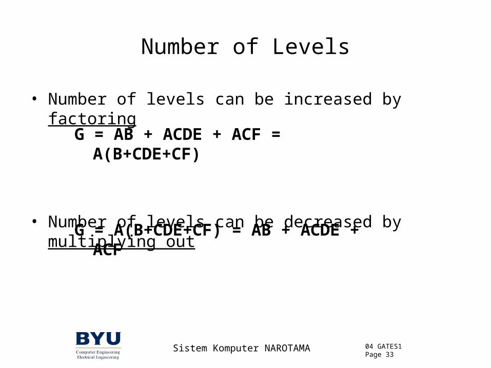
Number of Levels
• Number of levels can be increased by factoring
• Number of levels can be decreased by multiplying out
G = AB + ACDE + ACF = A(B+CDE+CF)
G = A(B+CDE+CF) = AB + ACDE + ACF

04 GATES1 Page 34
Sistem Komputer NAROTAMA
Example
G = AB + ACDE + ACFLevels = 2#Gates = 4Delay = tAND4 + tOR3
#Inputs = 12#transistors = 24Largest gate = 4 inputs
Area Calculations: - each input to a gate costs ~2 transistors - area # of transistorsDelay Calculations: - find slowest path from inputs to output
tdelay = tAND4 + tOR3
- the 4-input AND is likely slower than the other AND gates
A
B
ACDE
ACF
G

04 GATES1 Page 35
Sistem Komputer NAROTAMA
Change the number of levels by factoring
G = ACDE + ACF + AB = A(CDE + CF + B)
CDE
C
F
BA
G
Levels = 3#Gates = 4Delay = tAND3 + tOR3 + tAND2
#Inputs = 10#transistors = 20Largest gate = 3 inputs
factor
This is a 3-level circuit…

04 GATES1 Page 36
Sistem Komputer NAROTAMA
Factor Again
G = A(CDE + CF + B) = A[B+C(F+DE)]
A
BC
F
D
E
G
Levels = 5#Gates = 5Delay = 3 x tAND2 + 2 x tOR2
#Inputs = 10#transistors = 20Largest gate = 2 inputs
factor
This is a 5-level circuit…

04 GATES1 Page 37
Sistem Komputer NAROTAMA
Changing the number of levels
Three alternative solutions for same function…
2-level 3-level 5-level
Logic Levels 2 3 5Delay tAND4 + tOR3 tAND3 + tOR3 + tAND2 3 x tAND2 + 2 x tOR2
Gate Count 4 4 5Gate Inputs 12 10 10Transistors 24 20 20
Largest Gate 4 3 2
Each has different area/speed characteristics

04 GATES1 Page 38
Sistem Komputer NAROTAMA
Two-Level vs. Multi-Level
• In general:– two-level is fastest– multi-level can be smaller
• Exploring by hand to find just the right solution can be difficult
• We will focus on two-level– easy to get from truth table– minimization techniques in later chapters focus on
it

![b Part 1 [exterior]](https://static.fdocuments.pl/doc/165x107/6189531ba275e438a019e4e1/b-part-1-exterior.jpg)


![[2] CE 124 part 1](https://static.fdocuments.pl/doc/165x107/577d279f1a28ab4e1ea45fa6/2-ce-124-part-1.jpg)