Digital Realization of a Click Modulator for an Audio ...
5
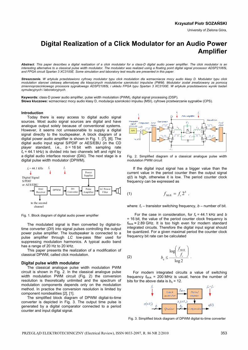
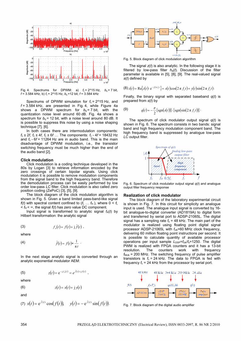
PRZEGLĄD ELEKTROTECHNICZNY (Electrical Review), ISSN 0033-2097, R. 86 NR 2/2010 353 Krzysztof Piotr SOZAŃSKI University of Zielona Góra, Digital Realization of a Click Modulator for an Audio Power Amplifier Abstract. This paper describes a digital realization of a click modulator for a class-D digital audio power amplifier. The click modulator is an interesting alternative to a classical pulse width modulator. The modulator was realized using a floating point digital signal processor ADSP21065L and FPGA circuit Spartan 3 XC3100E. Some simulation and laboratory test results are presented in this paper. Streszczenie. W artykule przedstawiono cyfrowy modulator typu click modulation dla wzmacniacza mocy audio klasy D. Modulator typu click modulation stanowi ciekawą alternatywę dla klasycznych modulatorów szerokości impulsów (PWM). Modulator został zrealizowany za pomocą zmiennoprzecinkowego procesora sygnałowego ADSP21065L i układu FPGA typu Spartan 3 XC3100E. W artykule przedstawiono wyniki badań symulacyjnych i laboratoryjnych. Keywords: class-D power audio amplifier, pulse width modulation (PWM), digital signal processing (DSP). Słowa kluczowe: wzmacniacz mocy audio klasy D, modulacja szerokości impulsu (MSI), cyfrowe przetwarzanie sygnałów (CPS). Introduction Today there is easy access to digital audio signal sources. Most audio signal sources are digital and have analogue output solely because of conventional systems. However, it seems not unreasonable to supply a digital signal directly to the loudspeaker. A block diagram of a digital power audio amplifier is shown in Fig. 1. [7], [6]. The digital audio input signal S/PDIF or AES/EBU (in the CD player standard, i.e., b = 16 bit with sampling rate f s = 44.1 kHz) is divided into two channels left and right by a digital audio interface receiver (DAI). The next stage is a digital pulse width modulator (DPWM). DPWM Digital Signal S/PDIF or AES/EBU f s D/t Converter Pulse Amplifier DAI Receiver f s fs = 44.1 kHz to the second channel LC Power Filter Power Supplier Fig. 1. Block diagram of digital audio power amplifier The modulated signal is then converted by digital-to- time converter (D/t) into signal pulses controlling the output power pulse amplifier. The loudspeaker is connected to a pulse amplifier through LC low-pass filter used for suppressing modulation harmonics. A typical audio band has a range of 20 Hz to 20 kHz. This paper presents the realization of a modification of classical DPWM, called click modulation. Digital pulse width modulator The classical analogue pulse width modulation PWM circuit is shown in Fig. 2. In the classical analogue pulse width modulation PWM circuit (Fig. 2) the conversion resolution is theoretically unlimited and the spectrum of modulation components depends only on the modulation method. In practice the conversion resolution is limited by component nonidealities [2], [1]. The simplified block diagram of DPWM digital-to-time converter is depicted in Fig. 3. The output time pulse is generated by a digital comparator connected to a period counter and input digital signal. Fig. 2. Simplified diagram of a classical analogue pulse width modulation PWM circuit If the digital input signal has a bigger value than the current value in the period counter then the output signal q(t) is high, otherwise it is low. The period counter clock frequency can be expressed as (1) b c Mclk f f 2 , where: f c – transistor switching frequency, b – number of bit. For the case in consideration, for f s = 44.1 kHz and b = 16 bit, the value of the period counter clock frequency is f Mclk ≈ 2.89 GHz. It is too high even for modern standard integrated circuits. Therefore the digital input signal should be quantized. For a given maximal period the counter clock frequency bit rate can be calculated (2) 2 log log c Mclk q f f b . For modern integrated circuits a value of switching frequency f Mclk = 200 MHz is usual, hence the number of bits for the above data is b q = 12. Fig. 3. Simplified block diagram of DPWM digital-to-time converter
Transcript of Digital Realization of a Click Modulator for an Audio ...
PRZEGLĄD ELEKTROTECHNICZNY (Electrical Review), ISSN 0033-2097, R. 86 NR 2/2010 353
Krzysztof Piotr SOZAŃSKI
University of Zielona Góra,
Digital Realization of a Click Modulator for an Audio Power Amplifier
Abstract. This paper describes a digital realization of a click modulator for a class-D digital audio power amplifier. The click modulator is an interesting alternative to a classical pulse width modulator. The modulator was realized using a floating point digital signal processor ADSP21065L and FPGA circuit Spartan 3 XC3100E. Some simulation and laboratory test results are presented in this paper. Streszczenie. W artykule przedstawiono cyfrowy modulator typu click modulation dla wzmacniacza mocy audio klasy D. Modulator typu click modulation stanowi ciekawą alternatywę dla klasycznych modulatorów szerokości impulsów (PWM). Modulator został zrealizowany za pomocą zmiennoprzecinkowego procesora sygnałowego ADSP21065L i układu FPGA typu Spartan 3 XC3100E. W artykule przedstawiono wyniki badań symulacyjnych i laboratoryjnych. Keywords: class-D power audio amplifier, pulse width modulation (PWM), digital signal processing (DSP). Słowa kluczowe: wzmacniacz mocy audio klasy D, modulacja szerokości impulsu (MSI), cyfrowe przetwarzanie sygnałów (CPS). Introduction
Today there is easy access to digital audio signal sources. Most audio signal sources are digital and have analogue output solely because of conventional systems. However, it seems not unreasonable to supply a digital signal directly to the loudspeaker. A block diagram of a digital power audio amplifier is shown in Fig. 1. [7], [6]. The digital audio input signal S/PDIF or AES/EBU (in the CD player standard, i.e., b = 16 bit with sampling rate fs = 44.1 kHz) is divided into two channels left and right by a digital audio interface receiver (DAI). The next stage is a digital pulse width modulator (DPWM).
DPWM
Digital Signal S/PDIF or AES/EBU
fs
D/t Converter
Pulse Amplifier
DAI Receiver
fs fs = 44.1 kHz
to the second channel
LC Power Filter
Power Supplier
Fig. 1. Block diagram of digital audio power amplifier
The modulated signal is then converted by digital-to-time converter (D/t) into signal pulses controlling the output power pulse amplifier. The loudspeaker is connected to a pulse amplifier through LC low-pass filter used for suppressing modulation harmonics. A typical audio band has a range of 20 Hz to 20 kHz.
This paper presents the realization of a modification of classical DPWM, called click modulation.
Digital pulse width modulator The classical analogue pulse width modulation PWM
circuit is shown in Fig. 2. In the classical analogue pulse width modulation PWM circuit (Fig. 2) the conversion resolution is theoretically unlimited and the spectrum of modulation components depends only on the modulation method. In practice the conversion resolution is limited by component nonidealities [2], [1].
The simplified block diagram of DPWM digital-to-time converter is depicted in Fig. 3. The output time pulse is generated by a digital comparator connected to a period counter and input digital signal.
Fig. 2. Simplified diagram of a classical analogue pulse width modulation PWM circuit
If the digital input signal has a bigger value than the
current value in the period counter then the output signal q(t) is high, otherwise it is low. The period counter clock frequency can be expressed as
(1) bcMclk ff 2 ,
where: fc – transistor switching frequency, b – number of bit.
For the case in consideration, for fs = 44.1 kHz and b = 16 bit, the value of the period counter clock frequency is fMclk ≈ 2.89 GHz. It is too high even for modern standard integrated circuits. Therefore the digital input signal should be quantized. For a given maximal period the counter clock frequency bit rate can be calculated
(2) 2log
log
c
Mclk
q
f
f
b .
For modern integrated circuits a value of switching frequency fMclk = 200 MHz is usual, hence the number of bits for the above data is bq = 12.
Fig. 3. Simplified block diagram of DPWM digital-to-time converter
354 PRZEGLĄD ELEKTROTECHNICZNY (Electrical Review), ISSN 0033-2097, R. 86 NR 2/2010
0 0.5 1 1.5 2 2.5 3 3.5 4 4.5 5x 10⁴
-100
-80
-60
-40
-20
0
Frequency [Hz]
Ma
gn
itu
de
[d
B]
a)
0 0.5 1 1.5 2 2.5 3 3.5 4 4.5 5x 10⁴
-100
-80
-60
-40
-20
0
Frequency [Hz]
Ma
gn
itu
de
[d
B]
b)
Fig. 4. Spectrums for DPWM: a) fc = 2^15 Hz, bq = 7 bit, f = 3.584 kHz, b) fc = 2^15 Hz, bq =12 bit, f = 3.584 kHz
Spectrums of DPWM simulation for fc = 2^15 Hz, and f = 3.584 kHz, are presented in Fig. 4, while Figure 4a shows a DPWM spectrum for bq = 7 bit, with the quantization noise level around 60 dB. Fig. 4a shows a spectrum for bq = 12 bit, with a noise level around 80 dB. It is possible to suppress this noise by using a noise shaping technique [7], [6].
In both cases there are intermodulation components: fc ± 2f, fc ± 4f, fc ± 6f … The components: fc - 4f = 18432 Hz and fc - 6f = 11264 Hz are in audio band. This is the main disadvantage of DPWM modulation, i.e., the transistor switching frequency must be much higher than the end of the audio band [2].
Click modulation Click modulation is a coding technique developed in the
80s by Logan [3] to retrieve information encoded by the zero crossings of certain bipolar signals. Using click modulation it is possible to remove modulation components from the signal band to the high frequency band. Therefore the demodulation process can be easily performed by low order low-pass LC filter. Click modulation is also called zero position coding (ZePoC) [3], [5], [9]. The block diagram of the click modulation algorithm is shown in Fig. 5. Given a band limited pass-band-like signal f(t) with spectral content confined to (fL … fH ), where 0 < fL < fH < ∞, the signal f(t) has zero value DC component.
Input signal is transformed to analytic signal fA(t) by Hilbert transformation: the analytic signal
(3) tftftf Aˆj ,
where
(4) t
tftfπ
1ˆ .
In the next stage analytic signal is converted through an analytic exponential modulator AEM:
(5) tftftf etz A jˆje ,
where
(6) tytxtz j
and
(7) tftytftx tftf sine ,cose )(ˆ)(ˆ .
Fig. 5. Block diagram of click modulation algorithm
The signal z(t) is also analytic. In the following stage it is filtered by low-pass filter ha(t). Discussion of the filter parameter is available in [5], [8], [9]. The real-valued signal s(t) defined by
(8) tftytftxtztz cctfc π2sinπ2coseRe π2j .
Finally, the binary signal with separated baseband q(t) is prepared from s(t) by
(9) tftstq cπ2sinsgnsgn2
.
The spectrum of click modulator output signal q(t) is shown in Fig. 6. The spectrum consists in two bands: signal band and high frequency modulation component band. The high frequency band is suppressed by analogue low-pass LC output filter.
fL fH
Spectrum of q(t)
0.5fc fc
|A|
f
1
SignalHigh
frequency component
Analog low-pass output filter
Fig. 6. Spectrum of click modulator output signal q(t) and analogue output filter frequency response Realization of click modulator The block diagram of the laboratory experimental circuit is shown in Fig. 7. In this circuit for simplicity an analogue input is used. The analogue input signal is converted by 16-bit analogue-to-digital converter (AD1819A) to digital form and transferred by serial port to ADSP-21065L. The digital signal has a sampling rate fs = 48 kHz. The main part of the modulator is realized using floating point digital signal processor ADSP-21065L with fclk=60 MHz clock frequency, delivering 60 million floating point instructions per second. It is possible to calculate quantity of available processor operations per input sample LDSP=fclk/fs=1250. The digital PWM is realized with FPGA counters and it has a 13-bit resolution. The counters work with frequency fMclk = 200 MHz. The switching frequency of pulse amplifier transistors is fc = 24 kHz. The data to FPGA is fed with frequency fc = 24 kHz from the processor by serial port.
Fig. 7. Block diagram of the digital audio amplifier
PRZEGLĄD ELEKTROTECHNICZNY (Electrical Review), ISSN 0033-2097, R. 86 NR 2/2010 355
The block diagram for the digital realization of the click modulator algorithm is presented in Fig. 10. Based on the linear phase response of the whole algorithm finite impulse response filters (FIR) have to be used. For Hilbert transformation of the input signal a FIR filter is applied. A practical FIR implementation of the Hilbert transformation will exhibit band-pass characteristics. The bottleneck of this algorithm is the low-frequency performance [5], [8]. The Hilbert FIR filter was designed using Matlab Signal Processing Toolbox, as shown in Listing 1. The frequency response of the Hilbert FIR filter (red line) and delay line (blue line) is depicted in Fig. 8. Realization of ADSP-21065L code for such FIR filter is described in Listing 2, with every filter tap executed in a single processor machine cycle. Similar to the Hilbert filter is the design of the Ha(z) FIR filter. Listing 1. Matlab program of interpolator FIR filter design
M = 120; % Order F = [0.02 0.98]; % Frequency Vector A = [1 1]; % Amplitude Vector W = 1; % Weight Vector b = remez(M, F, A, W, ’hilbert’) ;
0 0.5 1 1.5 2x 10⁴
-80
-60
-40
-20
0
Frequency [Hz]
Ma
gn
itu
de
[d
B]
a)
0 0.5 1 1.5 2x 10⁴
0
20
40
60
80
100
Frequency [Hz]
Ph
ase
[d
eg
]
b)
Fig. 8. Frequency responses of the Hilbert FIR filter (red line) and delay line (blue line): a) amplitude responses, b) difference of phase responses
The block diagram of digital signal interpolator is shown in Fig. 9. The input signal sampling rate is expanded by interleaving R-1 zero samples between every input sample.
In the next stage low-pass filter suppresses the aliasing components. Listing 2. The ADSP-21065L code for FIR filter realization
/* load sample from circular buffer in data memory and coefficient from circular buffer in program memory */ f2 = dm(i0, m0), f4 = pm(i8, m8); /* loop initialization */ lcntr = TAPS1−1, do (pc, 1) until lce; /* calculate filter tap */ f8 = f2 * f4 , f12 = f8+f12 , f2 = dm(i0, m0), f4 = pm(i8, m8); /* calculate last tap */ f8 = f2 * f4 , f12 = f8+f12; /* last accumulation */ f12 = f8+f12;
In practice, the low-pass filter should sufficiently attenuate the stopband to suppress the unwanted images of the baseband. Finally the signal amplitude is increased R times to compensate amplitude losses.
Fig. 9. Block diagram of signal interpolator In the designed modulator the finite impulse response filter FIR has to be used according to its linear phase response. The chosen interpolator ratio is R = 8. The FIR filter was designed using Matlab Signal Processing Toolbox as shown in Listing 3. The filter order is Nint = 127. Listing 3. Matlab program of interpolator FIR filter design
fp =48000*8; M = 127−1; % filter order Fpass = 12000; % passband Frequency Fstop = 30000; % stopband Frequency Wpass = 1; % passband Weight Wstop = 1; % stopband Weight b = firls(M, [0 Fpass Fstop fp/2]/(fp/2), [1 1 0 0], [Wpass Wstop]);
Fig. 10. Block diagram of digital realization of click modulator algorithm
356 PRZEGLĄD ELEKTROTECHNICZNY (Electrical Review), ISSN 0033-2097, R. 86 NR 2/2010
0 2 4 6 8 10 12 14 16 18x 104
-200
-150
-100
-50
0
Frequency [Hz]
Ma
gn
itu
de
[d
B]
a)
0 2 4 6 8 10 12 14 16 18x 104
-200
-150
-100
-50
0
Frequency [Hz]
Ma
gn
itu
de
[d
B]
b )
Fig. 11. Spectrums of the signals in the interpolator for R = 8 and 12 kHz input sinusoidal signal: a) spectrum of expanded signal, b) frequency response of the FIR filter and spectrum of output signal The spectrums of interpolator signals using such a FIR filter for 12 kHz sinusoidal input signal is shown in Fig. 11. The spectrum of the expanded signal is depicted in Fig. 11a. The output signal spectrum and the filter frequency response is presented in Fig. 11b. The designed interpolator requires Lint = Nint·R multiplication and addition per one input sample. It is possible to decrease the quantity of arithmetic calculation by elimination of the multiplication and addition for zero value samples. The block diagram of such solution is shown in Fig. 12 [7]. This is a FIR based signal interpolator for R = 8 with periodically switched coefficients and filter order Nint = 127. In this case the interpolator requires Lint = Nint multiplication and addition per one input signal sample. The modulator signal q(kTs/R) has a sampling rate equal to 384 kHz. This time resolution is too low to perform high quality audio signal. Therefore zero crossing point has to be calculated with higher accuracy. The FPGA counters work with a clock frequency equal to 200 MHz. The zero crossing point is calculated using linear interpolation [4]. This process is shown in Fig. 13. Experimental results The efficiency of the processor used for the realization of the modulator is not sufficient to support the entire algorithm at full speed (48 kHz), therefore signal band is limited to 12 kHz and transistor switching frequency is 24 kHz.
Y(z)
z-1
fs=48 kHz
z-1 z-1 X(z) R=8
h(0)
h(1)
h(2)
h(3)
h(4)
h(5)
h(6)
h(7)
h(9)
h(10)
h(11)
h(12)
h(13)
h(14)
h(15)
h(16)
h(17)
h(18)
h(19)
h(20)
h(21)
h(22)
h(23)
h(24)
h(120)
h(121)
h(122)
h(123)
h(124)
h(125)
h(126)
h(127)
Rfs=384kHz 1 2 3 16 ...
Fig. 12. Block diagram of FIR based signal interpolator for R=8 with periodically switched coefficients and filter order Nint = 127
),( 00 yx
),( 11 yx
2x
)2sin( cf
)( 2Tns
MHz200
1
kHz24
1
kHz24
1
MHzn
200
1
kHz488
1
)(kTq
Fig. 13. Zero crossing calculation
The click modulator is a big challenge for the processor, for example, Streitenberger et al. [8] used three processors with computational power 233 MMACs and two FPGAs. The click modulator circuit with pulse amplifier is shown in Fig. 14, and was tested in our Institute laboratory. A block diagram of the test circuit is presented in Fig. 15. Measurements were made using the computer controlled system Clio from Audiomatica. According to its advanced signal processing methods, it is possible to measure many electroacoustic parameters. Unfortunately this author has only access to the oldest version of such system with an 18-bit analogue-to-digital converter and a sampling rate of 48 kHz. It has too small a sampling rate to fully analyze such an amplifier, having a measuring band limited to 24 kHz. However it is possible to analyze the modulator limited to the 12 KHz band. The best solution for measurement problems is the system Two from Audio Precision. Experimental results for the sinusoidal input signal are presented in Fig. 16. The spectrum of the output signal for an input signal of 5 kHz is shown in Fig. 16a. Modulation components are from a signal band of 300 Hz to 12 kHz, and some harmonics in the signal band are connected with limited time resolution. Similar results are obtained for an input signal frequency equal 1 kHz (Fig. 16b). Frequency responses are shown in Fig. 17. The first one is made using stepped sinusoidal signal (Fig. 17a) and the second one using multitone sinusoidal signal (Fig. 17b). In both case results are similar.
Fig. 14. The click modulator with pulse amplifier
PRZEGLĄD ELEKTROTECHNICZNY (Electrical Review), ISSN 0033-2097, R. 86 NR 2/2010 357
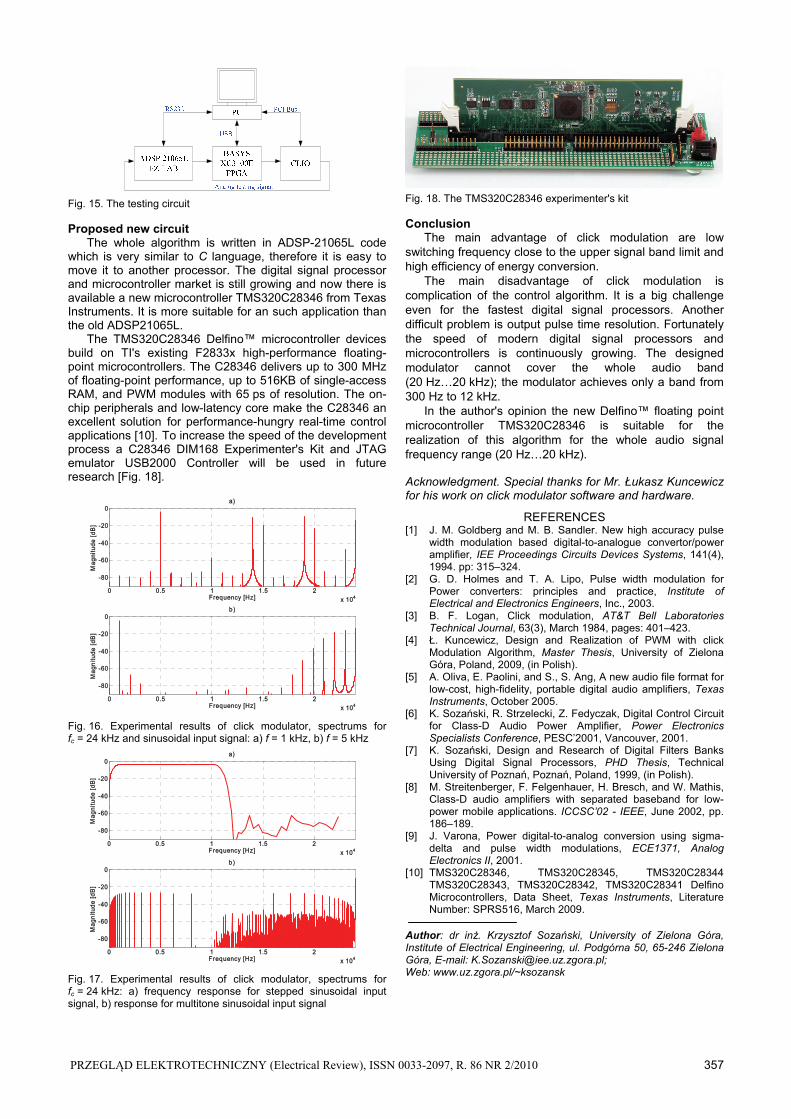
Fig. 15. The testing circuit Proposed new circuit The whole algorithm is written in ADSP-21065L code which is very similar to C language, therefore it is easy to move it to another processor. The digital signal processor and microcontroller market is still growing and now there is available a new microcontroller TMS320C28346 from Texas Instruments. It is more suitable for an such application than the old ADSP21065L. The TMS320C28346 Delfino™ microcontroller devices build on TI's existing F2833x high-performance floating-point microcontrollers. The C28346 delivers up to 300 MHz of floating-point performance, up to 516KB of single-access RAM, and PWM modules with 65 ps of resolution. The on-chip peripherals and low-latency core make the C28346 an excellent solution for performance-hungry real-time control applications [10]. To increase the speed of the development process a C28346 DIM168 Experimenter's Kit and JTAG emulator USB2000 Controller will be used in future research [Fig. 18].
0 0.5 1 1.5 2x 10⁴
-80
-60
-40
-20
0
Frequency [Hz]
Ma
gn
itu
de
[d
B]
a)
0 0.5 1 1.5 2x 10⁴
-80
-60
-40
-20
0
Frequency [Hz]
Ma
gn
itu
de
[d
B]
b )
Fig. 16. Experimental results of click modulator, spectrums for fc = 24 kHz and sinusoidal input signal: a) f = 1 kHz, b) f = 5 kHz
0 0.5 1 1.5 2x 10⁴
-80
-60
-40
-20
0
Frequency [Hz]
Ma
gn
itu
de
[d
B]
a)
0 0.5 1 1.5 2x 10⁴
-80
-60
-40
-20
0
Frequency [Hz]
Ma
gn
itu
de
[d
B]
b )
Fig. 17. Experimental results of click modulator, spectrums for fc = 24 kHz: a) frequency response for stepped sinusoidal input signal, b) response for multitone sinusoidal input signal
Fig. 18. The TMS320C28346 experimenter's kit Conclusion
The main advantage of click modulation are low switching frequency close to the upper signal band limit and high efficiency of energy conversion.
The main disadvantage of click modulation is complication of the control algorithm. It is a big challenge even for the fastest digital signal processors. Another difficult problem is output pulse time resolution. Fortunately the speed of modern digital signal processors and microcontrollers is continuously growing. The designed modulator cannot cover the whole audio band (20 Hz…20 kHz); the modulator achieves only a band from 300 Hz to 12 kHz.
In the author's opinion the new Delfino™ floating point microcontroller TMS320C28346 is suitable for the realization of this algorithm for the whole audio signal frequency range (20 Hz…20 kHz).
Acknowledgment. Special thanks for Mr. Łukasz Kuncewicz for his work on click modulator software and hardware.
REFERENCES [1] J. M. Goldberg and M. B. Sandler. New high accuracy pulse
width modulation based digital-to-analogue convertor/power amplifier, IEE Proceedings Circuits Devices Systems, 141(4), 1994. pp: 315–324.
[2] G. D. Holmes and T. A. Lipo, Pulse width modulation for Power converters: principles and practice, Institute of Electrical and Electronics Engineers, Inc., 2003.
[3] B. F. Logan, Click modulation, AT&T Bell Laboratories Technical Journal, 63(3), March 1984, pages: 401–423.
[4] Ł. Kuncewicz, Design and Realization of PWM with click Modulation Algorithm, Master Thesis, University of Zielona Góra, Poland, 2009, (in Polish).
[5] A. Oliva, E. Paolini, and S., S. Ang, A new audio file format for low-cost, high-fidelity, portable digital audio amplifiers, Texas Instruments, October 2005.
[6] K. Sozański, R. Strzelecki, Z. Fedyczak, Digital Control Circuit for Class-D Audio Power Amplifier, Power Electronics Specialists Conference, PESC’2001, Vancouver, 2001.
[7] K. Sozański, Design and Research of Digital Filters Banks Using Digital Signal Processors, PHD Thesis, Technical University of Poznań, Poznań, Poland, 1999, (in Polish).
[8] M. Streitenberger, F. Felgenhauer, H. Bresch, and W. Mathis, Class-D audio amplifiers with separated baseband for low-power mobile applications. ICCSC’02 - IEEE, June 2002, pp. 186–189.
[9] J. Varona, Power digital-to-analog conversion using sigma-delta and pulse width modulations, ECE1371, Analog Electronics II, 2001.
[10] TMS320C28346, TMS320C28345, TMS320C28344 TMS320C28343, TMS320C28342, TMS320C28341 Delfino Microcontrollers, Data Sheet, Texas Instruments, Literature Number: SPRS516, March 2009.
Author: dr inż. Krzysztof Sozański, University of Zielona Góra, Institute of Electrical Engineering, ul. Podgórna 50, 65-246 Zielona Góra, E-mail: [email protected]; Web: www.uz.zgora.pl/~ksozansk