Dobór pytań w metodzie zliczania odpowiedzi ( Item Count Method ).
Nonpolar GaN substrates grown by ammonothermal methodR. Kucharski, M. Rudziński, M. Zając, R. Doradziński, J. Garczyński, L. Sierzputowski, R. Kudrawiec, J.Serafińczuk, W. Strupiński, and R. Dwiliński Citation: Applied Physics Letters 95, 131119 (2009); doi: 10.1063/1.3227893 View online: http://dx.doi.org/10.1063/1.3227893 View Table of Contents: http://scitation.aip.org/content/aip/journal/apl/95/13?ver=pdfcov Published by the AIP Publishing Articles you may be interested in Contactless electroreflectance of AlGaN/GaN heterostructures deposited on c-, a-, m-, and (20.1)-plane GaNbulk substrates grown by ammonothermal method J. Appl. Phys. 109, 063528 (2011); 10.1063/1.3560537 Application of contactless electroreflectance to study the epi readiness of m -plane GaN substrates obtainedby ammonothermal method J. Vac. Sci. Technol. A 28, L18 (2010); 10.1116/1.3504359 Contactless electroreflectance of GaN bulk crystals grown by ammonothermal method and GaN epilayersgrown on these crystals Appl. Phys. Lett. 93, 061910 (2008); 10.1063/1.2972030 Contactless electroreflectance, in the range of 20 K K , of freestanding wurtzite GaN prepared by hydride-vapor-phase epitaxy J. Appl. Phys. 94, 899 (2003); 10.1063/1.1582230 Optical properties of GaN epilayers and GaN/AlGaN quantum wells grown by molecular beam epitaxy onGaN(0001) single crystal substrate J. Appl. Phys. 88, 183 (2000); 10.1063/1.373640
This article is copyrighted as indicated in the article. Reuse of AIP content is subject to the terms at: http://scitation.aip.org/termsconditions. Downloaded to IP:
130.18.123.11 On: Thu, 18 Dec 2014 15:40:03
Nonpolar GaN substrates grown by ammonothermal methodR. Kucharski,1 M. Rudziński,2 M. Zając,1,a� R. Doradziński,1 J. Garczyński,1
L. Sierzputowski,1 R. Kudrawiec,3 J. Serafińczuk,4 W. Strupiński,2 and R. Dwiliński11AMMONO Sp. z o.o., Czerwonego Krzyża 2/31, 00-377 Warsaw, Poland2Institute of Electronic Materials Technology, Wólczyńska 133, 01-919 Warsaw, Poland3Institute of Physics, Wrocław University of Technology, Wybrzeże Wyspiańskiego 27,50-370 Wrocław, Poland4Faculty of Microsystem Electronics and Photonics, Wrocław University of Technology,Janiszewskiego 11/17, 50-372 Wrocław, Poland
�Received 21 July 2009; accepted 29 July 2009; published online 2 October 2009�
In this letter, the authors demonstrate large size m-plane GaN substrates grown by ammonothermalmethod. These substrates have excellent structural quality. The concentration of threadingdislocation density is below 5�104 cm−2 and the full width at half maximum for the symmetricaland asymmetrical peaks equals 16 and 19 arc sec, respectively. Also good optical quality, the energygap-related transition is clearly observed at room temperature in photoluminescence and contactlesselectroreflectance spectra. GaN epilayers deposited on these substrates exhibit intrinsic narrowexciton lines which are very sensitive to the optical selection rules typical for hexagonal symmetry,proving truly nonpolar character of the material. © 2009 American Institute of Physics.�doi:10.1063/1.3227893�
Because of no piezoelectric field along the �11̄00� and
�112̄0� direction in GaN crystals, m-plane GaN substrates ofhigh quality and large sizes are very desirable for epitaxy ofInGaN quantum wells �QWs� for photonics1 especially greenlasers.2 Recently, a large progress has been made in the de-velopment of the growth of truly bulk GaN crystals by am-monothermal method.3–7 High quality 2 in. c-plane GaN sub-strates have been presented by AMMONO company lastyear.3 Currently, 1 and 1.5 in. substrates are available on themarket.4 However, for photonic applications m-plane GaNsubstrates are more promising and interesting. Since nowsuch substrates have been obtained by hydride vapor phaseepitaxy �HVPE� method8,9 by slicing the c-direction grownbulk boule along the proper direction, yielding to about 1 cmsquare �13�8 mm2� plates. Similar approach was applied toGaN crystals grown by ammonothermal method. In this casethe larger size of semipolar or nonpolar GaN substrates canbe obtained from much smaller diameter of bulk boule, whencompare to 2 in. HVPE GaN. In this letter we presentm-plane GaN substrates of excellent quality which have beenrecently developed at the AMMONO company.
Ammonothermal synthesis of bulk GaN crystals�A-GaN� was already described elsewhere.4 This techniqueenables growth of crystals of large sizes, excellent crystallineproperties �full width half maximum for �00.2� x-ray diffrac-tion peak equals 17 arc sec�, with extremely flat crystal lat-tice �radius of curvature higher than 100 m� and very lowdislocation density ��5�103 cm−2�.4 This is a direct conse-quence of adapting the method of truly bulk GaN production,without necessity of using non-native seeds, contrary toHVPE method. Extremely flat crystal lattice of bulk boule inA-GaN is the largest advantage in producing nonpolar orsemipolar substrates. They are not limited in length due tothe lack of crystal bowing as it takes place in the crystalsproduced by HVPE. Moreover, ammonothermal technique is
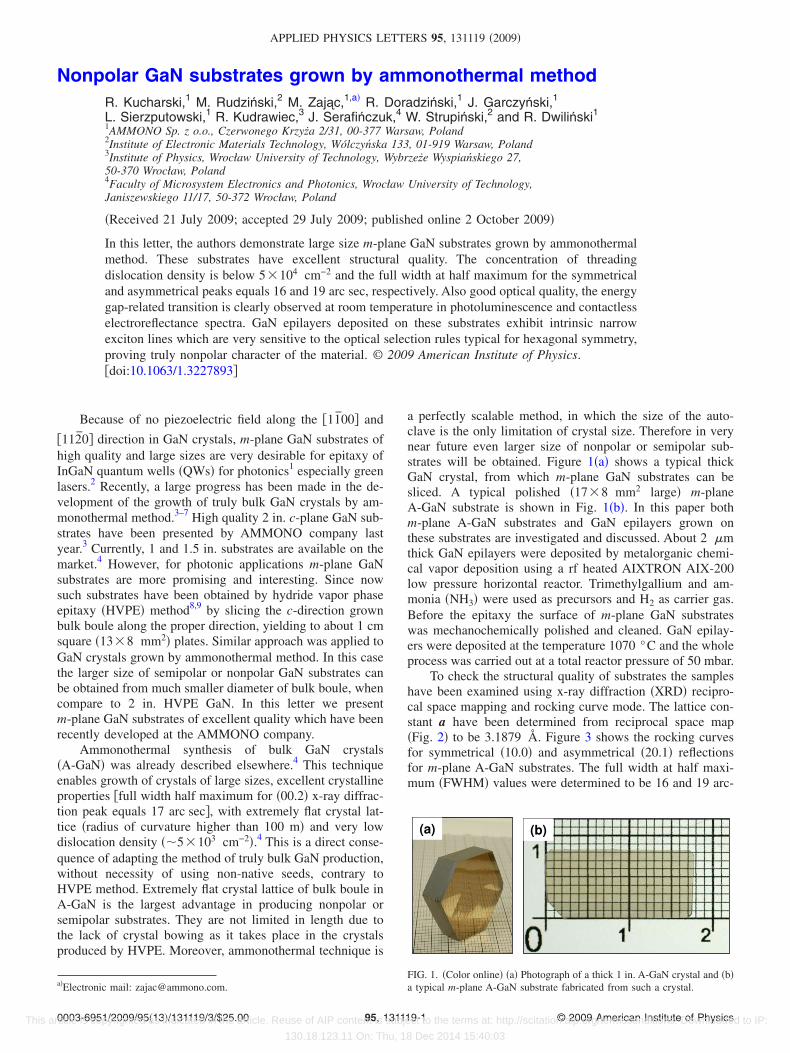
a perfectly scalable method, in which the size of the auto-clave is the only limitation of crystal size. Therefore in verynear future even larger size of nonpolar or semipolar sub-strates will be obtained. Figure 1�a� shows a typical thickGaN crystal, from which m-plane GaN substrates can besliced. A typical polished �17�8 mm2 large� m-planeA-GaN substrate is shown in Fig. 1�b�. In this paper bothm-plane A-GaN substrates and GaN epilayers grown onthese substrates are investigated and discussed. About 2 �mthick GaN epilayers were deposited by metalorganic chemi-cal vapor deposition using a rf heated AIXTRON AIX-200low pressure horizontal reactor. Trimethylgallium and am-monia �NH3� were used as precursors and H2 as carrier gas.Before the epitaxy the surface of m-plane GaN substrateswas mechanochemically polished and cleaned. GaN epilay-ers were deposited at the temperature 1070 °C and the wholeprocess was carried out at a total reactor pressure of 50 mbar.
To check the structural quality of substrates the sampleshave been examined using x-ray diffraction �XRD� recipro-cal space mapping and rocking curve mode. The lattice con-stant a have been determined from reciprocal space map�Fig. 2� to be 3.1879 Å. Figure 3 shows the rocking curvesfor symmetrical �10.0� and asymmetrical �20.1� reflectionsfor m-plane A-GaN substrates. The full width at half maxi-mum �FWHM� values were determined to be 16 and 19 arc-
a�Electronic mail: [email protected]. 1. �Color online� �a� Photograph of a thick 1 in. A-GaN crystal and �b�a typical m-plane A-GaN substrate fabricated from such a crystal.
APPLIED PHYSICS LETTERS 95, 131119 �2009�
0003-6951/2009/95�13�/131119/3/$25.00 © 2009 American Institute of Physics95, 131119-1 This article is copyrighted as indicated in the article. Reuse of AIP content is subject to the terms at: http://scitation.aip.org/termsconditions. Downloaded to IP:
130.18.123.11 On: Thu, 18 Dec 2014 15:40:03
sec for the symmetrical �10.0� and asymmetrical �20.1�peaks, respectively. These results strongly indicate excellentcrystalline quality of the studied material. This is the lowestFWHM value ever reported for HVPE m-plane orientedGaN. So far, Fujito et al.9 published 25–35 arc sec and Hash-imoto et al.5 presented 20–30 arc sec for nonpolar HVPEGaN crystals and ammonothermally grown GaN crystals ob-tained on HVPE seeds, respectively.
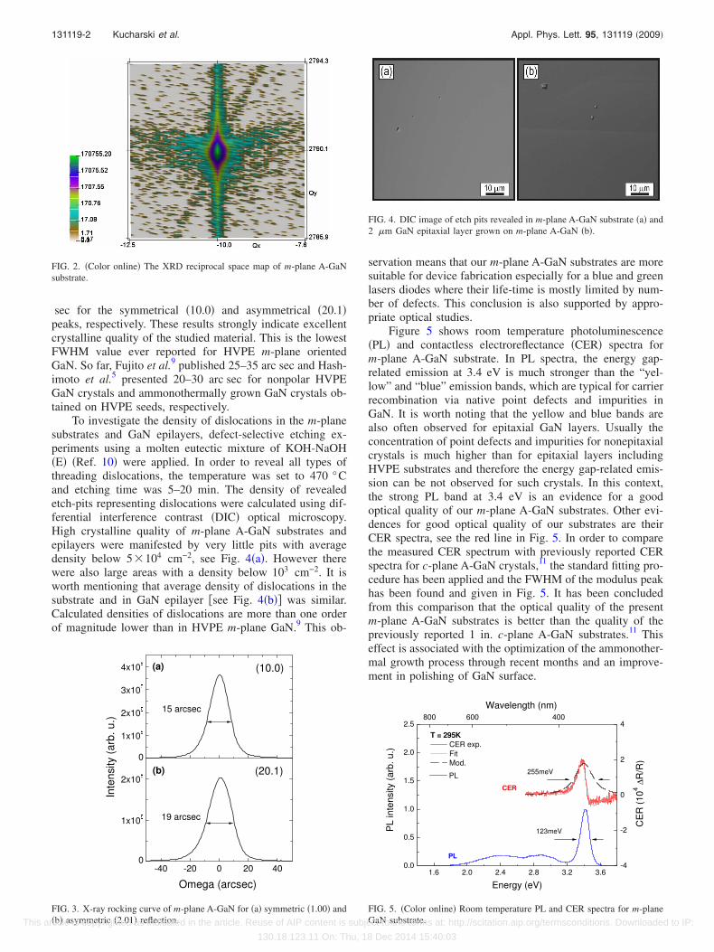
To investigate the density of dislocations in the m-planesubstrates and GaN epilayers, defect-selective etching ex-periments using a molten eutectic mixture of KOH-NaOH�E� �Ref. 10� were applied. In order to reveal all types ofthreading dislocations, the temperature was set to 470 °Cand etching time was 5–20 min. The density of revealedetch-pits representing dislocations were calculated using dif-ferential interference contrast �DIC� optical microscopy.High crystalline quality of m-plane A-GaN substrates andepilayers were manifested by very little pits with averagedensity below 5�104 cm−2, see Fig. 4�a�. However therewere also large areas with a density below 103 cm−2. It isworth mentioning that average density of dislocations in thesubstrate and in GaN epilayer �see Fig. 4�b�� was similar.Calculated densities of dislocations are more than one orderof magnitude lower than in HVPE m-plane GaN.9 This ob-
servation means that our m-plane A-GaN substrates are moresuitable for device fabrication especially for a blue and greenlasers diodes where their life-time is mostly limited by num-ber of defects. This conclusion is also supported by appro-priate optical studies.
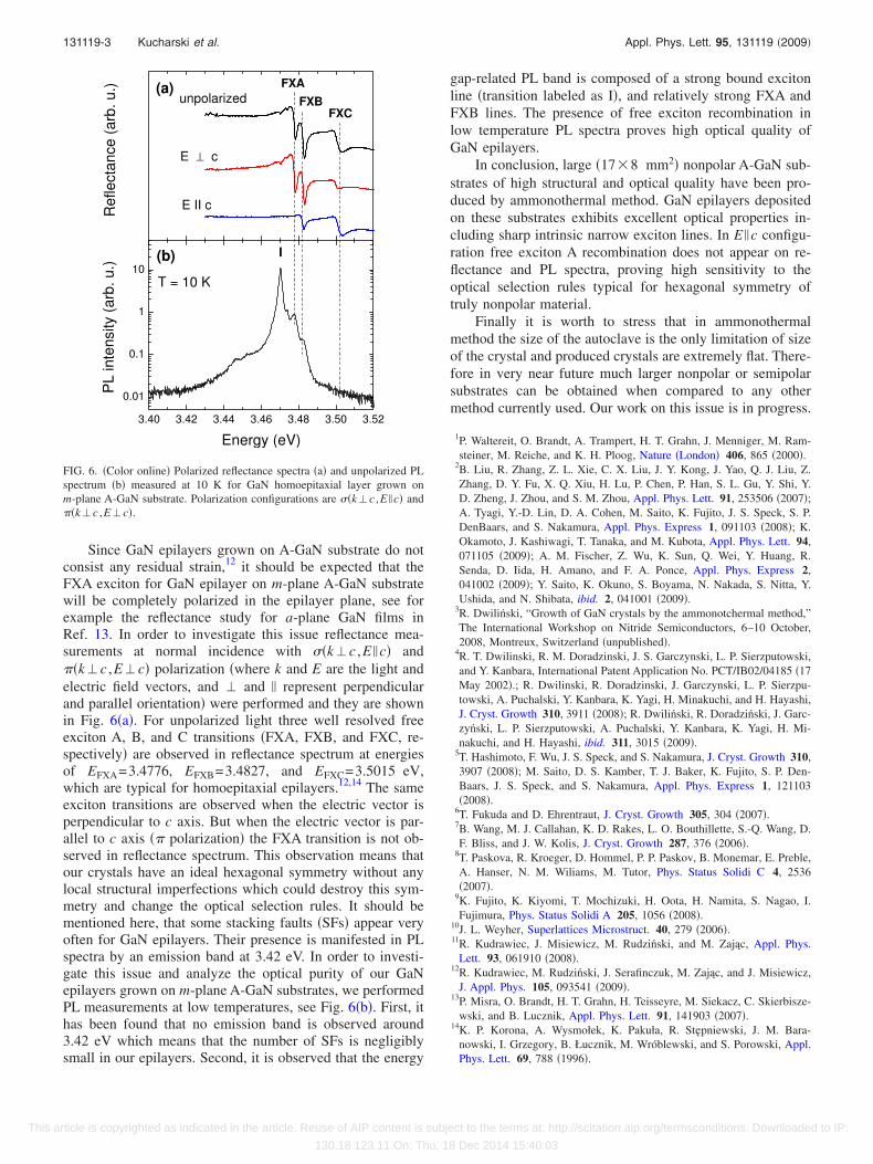
Figure 5 shows room temperature photoluminescence�PL� and contactless electroreflectance �CER� spectra form-plane A-GaN substrate. In PL spectra, the energy gap-related emission at 3.4 eV is much stronger than the “yel-low” and “blue” emission bands, which are typical for carrierrecombination via native point defects and impurities inGaN. It is worth noting that the yellow and blue bands arealso often observed for epitaxial GaN layers. Usually theconcentration of point defects and impurities for nonepitaxialcrystals is much higher than for epitaxial layers includingHVPE substrates and therefore the energy gap-related emis-sion can be not observed for such crystals. In this context,the strong PL band at 3.4 eV is an evidence for a goodoptical quality of our m-plane A-GaN substrates. Other evi-dences for good optical quality of our substrates are theirCER spectra, see the red line in Fig. 5. In order to comparethe measured CER spectrum with previously reported CERspectra for c-plane A-GaN crystals,11 the standard fitting pro-cedure has been applied and the FWHM of the modulus peakhas been found and given in Fig. 5. It has been concludedfrom this comparison that the optical quality of the presentm-plane A-GaN substrates is better than the quality of thepreviously reported 1 in. c-plane A-GaN substrates.11 Thiseffect is associated with the optimization of the ammonother-mal growth process through recent months and an improve-ment in polishing of GaN surface.
FIG. 2. �Color online� The XRD reciprocal space map of m-plane A-GaNsubstrate.
FIG. 3. X-ray rocking curve of m-plane A-GaN for �a� symmetric �1.00� and�b� asymmetric �2.01� reflection.
FIG. 4. DIC image of etch pits revealed in m-plane A-GaN substrate �a� and2 �m GaN epitaxial layer grown on m-plane A-GaN �b�.
FIG. 5. �Color online� Room temperature PL and CER spectra for m-planeGaN substrate.
131119-2 Kucharski et al. Appl. Phys. Lett. 95, 131119 �2009�
This article is copyrighted as indicated in the article. Reuse of AIP content is subject to the terms at: http://scitation.aip.org/termsconditions. Downloaded to IP:
130.18.123.11 On: Thu, 18 Dec 2014 15:40:03
Since GaN epilayers grown on A-GaN substrate do notconsist any residual strain,12 it should be expected that theFXA exciton for GaN epilayer on m-plane A-GaN substratewill be completely polarized in the epilayer plane, see forexample the reflectance study for a-plane GaN films inRef. 13. In order to investigate this issue reflectance mea-surements at normal incidence with ��k�c ,E �c� and��k�c ,E�c� polarization �where k and E are the light andelectric field vectors, and � and � represent perpendicularand parallel orientation� were performed and they are shownin Fig. 6�a�. For unpolarized light three well resolved freeexciton A, B, and C transitions �FXA, FXB, and FXC, re-spectively� are observed in reflectance spectrum at energiesof EFXA=3.4776, EFXB=3.4827, and EFXC=3.5015 eV,which are typical for homoepitaxial epilayers.12,14 The sameexciton transitions are observed when the electric vector isperpendicular to c axis. But when the electric vector is par-allel to c axis �� polarization� the FXA transition is not ob-served in reflectance spectrum. This observation means thatour crystals have an ideal hexagonal symmetry without anylocal structural imperfections which could destroy this sym-metry and change the optical selection rules. It should bementioned here, that some stacking faults �SFs� appear veryoften for GaN epilayers. Their presence is manifested in PLspectra by an emission band at 3.42 eV. In order to investi-gate this issue and analyze the optical purity of our GaNepilayers grown on m-plane A-GaN substrates, we performedPL measurements at low temperatures, see Fig. 6�b�. First, ithas been found that no emission band is observed around3.42 eV which means that the number of SFs is negligiblysmall in our epilayers. Second, it is observed that the energy
gap-related PL band is composed of a strong bound excitonline �transition labeled as I�, and relatively strong FXA andFXB lines. The presence of free exciton recombination inlow temperature PL spectra proves high optical quality ofGaN epilayers.
In conclusion, large �17�8 mm2� nonpolar A-GaN sub-strates of high structural and optical quality have been pro-duced by ammonothermal method. GaN epilayers depositedon these substrates exhibits excellent optical properties in-cluding sharp intrinsic narrow exciton lines. In E �c configu-ration free exciton A recombination does not appear on re-flectance and PL spectra, proving high sensitivity to theoptical selection rules typical for hexagonal symmetry oftruly nonpolar material.
Finally it is worth to stress that in ammonothermalmethod the size of the autoclave is the only limitation of sizeof the crystal and produced crystals are extremely flat. There-fore in very near future much larger nonpolar or semipolarsubstrates can be obtained when compared to any othermethod currently used. Our work on this issue is in progress.
1P. Waltereit, O. Brandt, A. Trampert, H. T. Grahn, J. Menniger, M. Ram-steiner, M. Reiche, and K. H. Ploog, Nature �London� 406, 865 �2000�.
2B. Liu, R. Zhang, Z. L. Xie, C. X. Liu, J. Y. Kong, J. Yao, Q. J. Liu, Z.Zhang, D. Y. Fu, X. Q. Xiu, H. Lu, P. Chen, P. Han, S. L. Gu, Y. Shi, Y.D. Zheng, J. Zhou, and S. M. Zhou, Appl. Phys. Lett. 91, 253506 �2007�;A. Tyagi, Y.-D. Lin, D. A. Cohen, M. Saito, K. Fujito, J. S. Speck, S. P.DenBaars, and S. Nakamura, Appl. Phys. Express 1, 091103 �2008�; K.Okamoto, J. Kashiwagi, T. Tanaka, and M. Kubota, Appl. Phys. Lett. 94,071105 �2009�; A. M. Fischer, Z. Wu, K. Sun, Q. Wei, Y. Huang, R.Senda, D. Iida, H. Amano, and F. A. Ponce, Appl. Phys. Express 2,041002 �2009�; Y. Saito, K. Okuno, S. Boyama, N. Nakada, S. Nitta, Y.Ushida, and N. Shibata, ibid. 2, 041001 �2009�.
3R. Dwiliński, “Growth of GaN crystals by the ammonotchermal method,”The International Workshop on Nitride Semiconductors, 6–10 October,2008, Montreux, Switzerland �unpublished�.
4R. T. Dwilinski, R. M. Doradzinski, J. S. Garczynski, L. P. Sierzputowski,and Y. Kanbara, International Patent Application No. PCT/IB02/04185 �17May 2002�.; R. Dwilinski, R. Doradzinski, J. Garczynski, L. P. Sierzpu-towski, A. Puchalski, Y. Kanbara, K. Yagi, H. Minakuchi, and H. Hayashi,J. Cryst. Growth 310, 3911 �2008�; R. Dwiliński, R. Doradziński, J. Garc-zyński, L. P. Sierzputowski, A. Puchalski, Y. Kanbara, K. Yagi, H. Mi-nakuchi, and H. Hayashi, ibid. 311, 3015 �2009�.
5T. Hashimoto, F. Wu, J. S. Speck, and S. Nakamura, J. Cryst. Growth 310,3907 �2008�; M. Saito, D. S. Kamber, T. J. Baker, K. Fujito, S. P. Den-Baars, J. S. Speck, and S. Nakamura, Appl. Phys. Express 1, 121103�2008�.
6T. Fukuda and D. Ehrentraut, J. Cryst. Growth 305, 304 �2007�.7B. Wang, M. J. Callahan, K. D. Rakes, L. O. Bouthillette, S.-Q. Wang, D.F. Bliss, and J. W. Kolis, J. Cryst. Growth 287, 376 �2006�.
8T. Paskova, R. Kroeger, D. Hommel, P. P. Paskov, B. Monemar, E. Preble,A. Hanser, N. M. Wiliams, M. Tutor, Phys. Status Solidi C 4, 2536�2007�.
9K. Fujito, K. Kiyomi, T. Mochizuki, H. Oota, H. Namita, S. Nagao, I.Fujimura, Phys. Status Solidi A 205, 1056 �2008�.
10J. L. Weyher, Superlattices Microstruct. 40, 279 �2006�.11R. Kudrawiec, J. Misiewicz, M. Rudziński, and M. Zając, Appl. Phys.
Lett. 93, 061910 �2008�.12R. Kudrawiec, M. Rudziński, J. Serafinczuk, M. Zając, and J. Misiewicz,
J. Appl. Phys. 105, 093541 �2009�.13P. Misra, O. Brandt, H. T. Grahn, H. Teisseyre, M. Siekacz, C. Skierbisze-
wski, and B. Lucznik, Appl. Phys. Lett. 91, 141903 �2007�.14K. P. Korona, A. Wysmołek, K. Pakuła, R. StJpniewski, J. M. Bara-
nowski, I. Grzegory, B. Łucznik, M. Wróblewski, and S. Porowski, Appl.Phys. Lett. 69, 788 �1996�.
FIG. 6. �Color online� Polarized reflectance spectra �a� and unpolarized PLspectrum �b� measured at 10 K for GaN homoepitaxial layer grown onm-plane A-GaN substrate. Polarization configurations are ��k�c ,E �c� and��k�c ,E�c�.
131119-3 Kucharski et al. Appl. Phys. Lett. 95, 131119 �2009�
This article is copyrighted as indicated in the article. Reuse of AIP content is subject to the terms at: http://scitation.aip.org/termsconditions. Downloaded to IP:
130.18.123.11 On: Thu, 18 Dec 2014 15:40:03