Sem short note 1
29
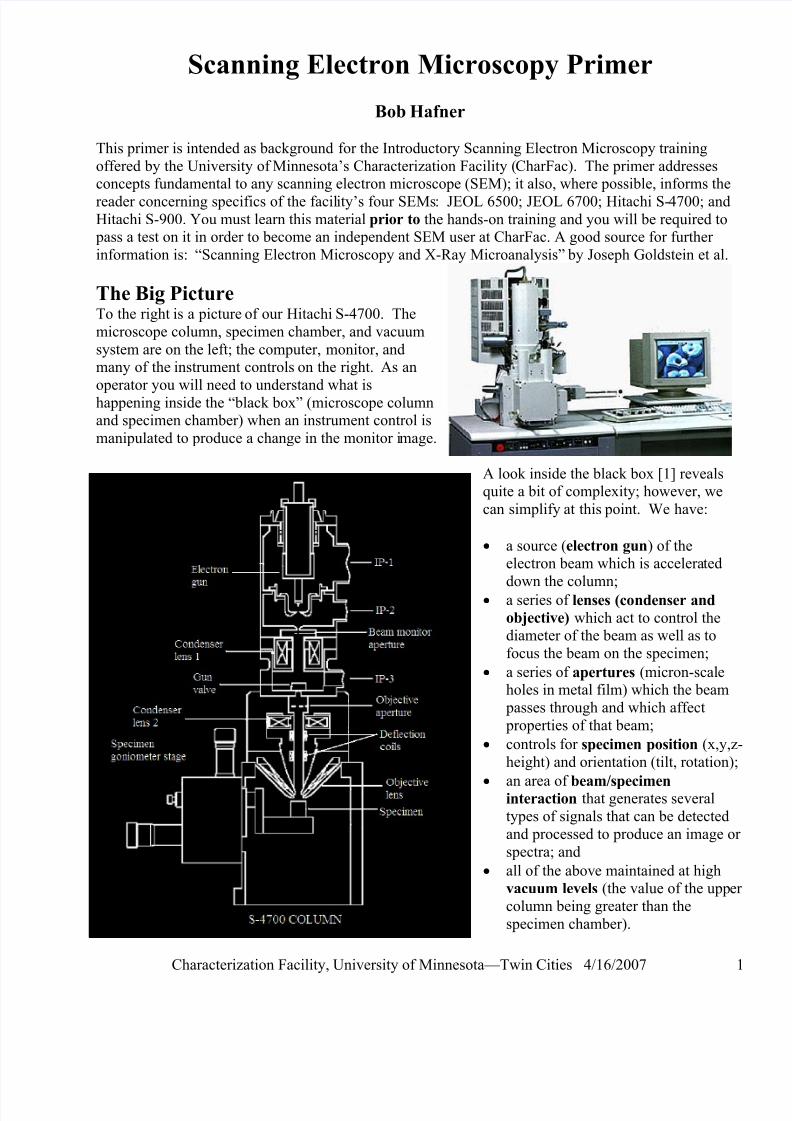
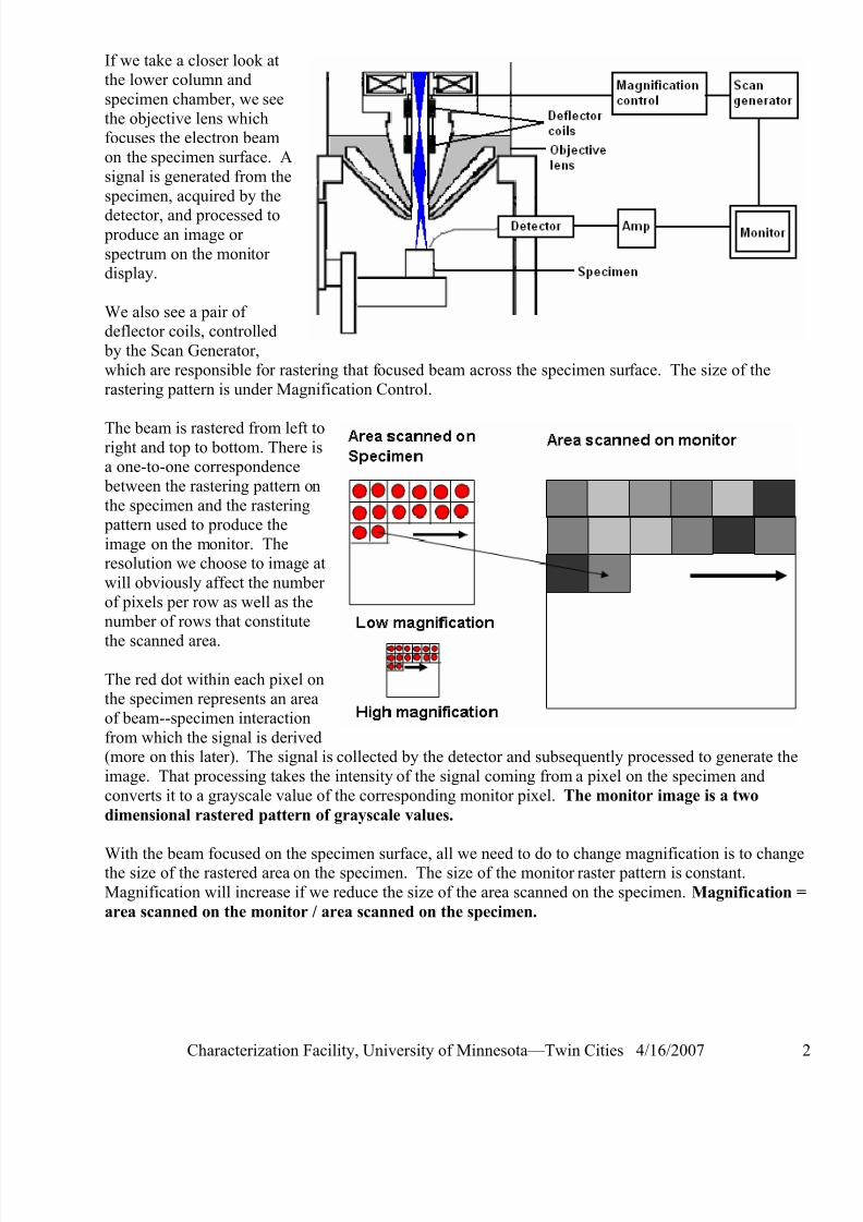
Scanning Electron Microscopy Primer Bob Hafner This primer is intended as background for the Introductory Scanning Electron Microscopy training offered by the University of Minnesota’s Characterization Facility ( CharFac). The primer addresses concepts fundamental to any scanning electron microscope (SEM); it also, where possible, informs the reader concerning specifics of the facility’s four SEMs: JEOL 6500; JEOL 6700; Hitachi S- 4700; and Hitachi S-900. You must learn this material prior to the hands-on training and you will be required to pass a test on it in order to become an independent SEM user at CharFac. A good source for further information is: “Scanning Electron Microscopy and X-Ray Microanalysis” by Joseph Goldstein et al. Characterization Facility, University of Minnesota—Twin Cities 4/16/2007 1 mage. A look inside the black box [1] reveals a source (electron gun) of the ted • ndenser and • e • (x,y,z- • veral • e maintained at high er The Big Picture To the right is a picture of our Hitachi S-4700. The microscope column, specimen chamber, and vacuum system are on the left; the computer, monitor, and many of the instrument controls on the right. As an operator you will need to understand what is happening inside the “black box” (microscope column and specimen chamber) when an instrument control is manipulated to produce a change in the monitor i quite a bit of complexity; however, we can simplify at this point. We have: • electron beam which is accelera down the column; a series of lenses (co objective) which act to control the diameter of the beam as well as to focus the beam on the specimen; a series of apertures (micron-scal holes in metal film) which the beam passes through and which affect properties of that beam; controls for specimen position height) and orientation (tilt, rotation); an area of beam/specimen interaction that generates se types of signals that can be detected and processed to produce an image or spectra; and all of the abov vacuum levels (the value of the upp column being greater than the specimen chamber).
-
Upload
mustaque-ali -
Category
Documents
-
view
220 -
download
0
Transcript of Sem short note 1
7/22/2019 Sem short note 1
http://slidepdf.com/reader/full/sem-short-note-1 1/29
Scanning Electron Microscopy Primer
Bob Hafner
This primer is intended as background for the Introductory Scanning Electron Microscopy training
offered by the University of Minnesota’s Characterization Facility (CharFac). The primer addressesconcepts fundamental to any scanning electron microscope (SEM); it also, where possible, informs the
reader concerning specifics of the facility’s four SEMs: JEOL 6500; JEOL 6700; Hitachi S-4700; andHitachi S-900. You must learn this material prior to the hands-on training and you will be required to pass a test on it in order to become an independent SEM user at CharFac. A good source for further
information is: “Scanning Electron Microscopy and X-Ray Microanalysis” by Joseph Goldstein et al.
Characterization Facility, University of Minnesota—Twin Cities 4/16/2007 1
mage.
A look inside the black box [1] reveals
a source (electron gun) of theted
• ndenser and
• e
• (x,y,z-
• veral
• e maintained at higher
The Big PictureTo the right is a picture of our Hitachi S-4700. The
microscope column, specimen chamber, and vacuum
system are on the left; the computer, monitor, andmany of the instrument controls on the right. As an
operator you will need to understand what is
happening inside the “black box” (microscope columnand specimen chamber) when an instrument control is
manipulated to produce a change in the monitor i
quite a bit of complexity; however, we
can simplify at this point. We have:
•
electron beam which is accelera
down the column;
a series of lenses (co
objective) which act to control thediameter of the beam as well as to
focus the beam on the specimen;
a series of apertures (micron-scalholes in metal film) which the beam
passes through and which affect
properties of that beam;
controls for specimen position
height) and orientation (tilt, rotation);
an area of beam/specimeninteraction that generates se
types of signals that can be detected
and processed to produce an image or
spectra; and
all of the abov
vacuum levels (the value of the upp
column being greater than the
specimen chamber).
7/22/2019 Sem short note 1
http://slidepdf.com/reader/full/sem-short-note-1 2/29
Characterization Facility, University of Minnesota—Twin Cities 4/16/2007 2
we take a closer look at
see
tor
e also see a pair ofled
r rastering that focused beam across the specimen surface. The size of the
he beam is rastered from left to
n
e at
he red dot within each pixel on
collected by the detector and subsequently processed to generate the
ith the beam focused on the specimen surface, all we need to do to change magnification is to change
ation =
If the lower column and
specimen chamber, we
the objective lens whichfocuses the electron beam
on the specimen surface. A
signal is generated from the
specimen, acquired by the
detector, and processed to produce an image or
spectrum on the monidisplay.
Wdeflector coils, control
by the Scan Generator,
which are responsible fo
rastering pattern is under Magnification Control.
Tright and top to bottom. There isa one-to-one correspondence
between the rastering pattern o
the specimen and the rastering pattern used to produce the
image on the monitor. Theresolution we choose to imag
will obviously affect the number
of pixels per row as well as thenumber of rows that constitute
the scanned area.
Tthe specimen represents an area
of beam--specimen interaction
from which the signal is derived(more on this later). The signal is
image. That processing takes the intensity of the signal coming from a pixel on the specimen and
converts it to a grayscale value of the corresponding monitor pixel. The monitor image is a two
dimensional rastered pattern of grayscale values.
Wthe size of the rastered area on the specimen. The size of the monitor raster pattern is constant.
Magnification will increase if we reduce the size of the area scanned on the specimen. Magnific
area scanned on the monitor / area scanned on the specimen.
7/22/2019 Sem short note 1
http://slidepdf.com/reader/full/sem-short-note-1 3/29
Characterization Facility, University of Minnesota—Twin Cities 4/16/2007 3
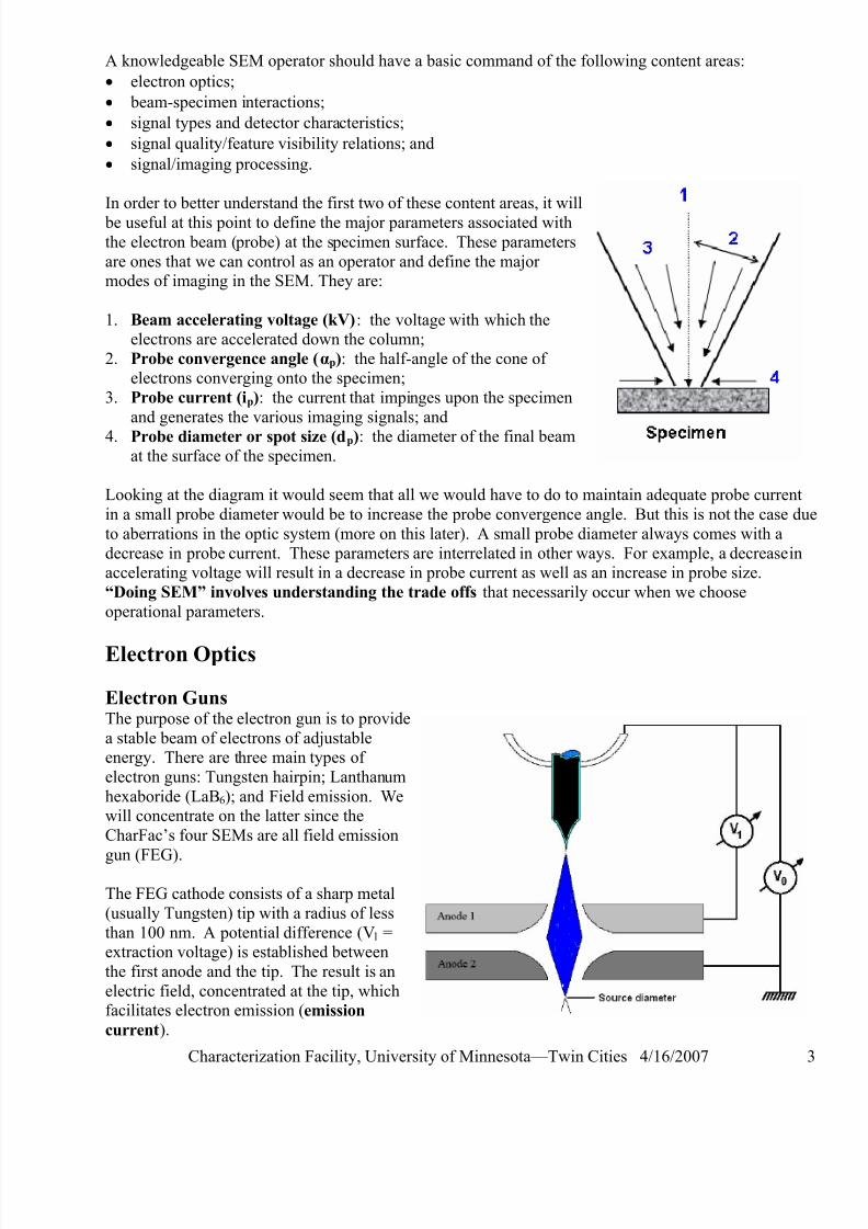
knowledgeable SEM operator should have a basic command of the following content areas:
nteractions;
cteristics;
nd
order to better understand the first two of these content areas, it will
Beam accelerating voltage (kV): the voltage with which the
2. le of the cone of
3. ges upon the specimen
4. of the final beam
ooking at the diagram it would seem that all we would have to do to maintain adequate probe current
in
lectron Optics
lectron Gunselectron gun is to provide
e
um
e
he FEG cathode consists of a sharp metal
A
• electron optics;
• beam-specimen i
• signal types and detector chara
• signal quality/feature visibility relations; a
• signal/imaging processing.
In
be useful at this point to define the major parameters associated with
the electron beam (probe) at the specimen surface. These parameters
are ones that we can control as an operator and define the majormodes of imaging in the SEM. They are:
1.electrons are accelerated down the column;
Probe convergence angle (αp): the half-angelectrons converging onto the specimen;
Probe current (ip): the current that impin
and generates the various imaging signals; and
Probe diameter or spot size (dp): the diameterat the surface of the specimen.
L
in a small probe diameter would be to increase the probe convergence angle. But this is not the case due
to aberrations in the optic system (more on this later). A small probe diameter always comes with a
decrease in probe current. These parameters are interrelated in other ways. For example, a decreaseaccelerating voltage will result in a decrease in probe current as well as an increase in probe size.
“Doing SEM” involves understanding the trade offs that necessarily occur when we choose
operational parameters.
E
EThe purpose of the
a stable beam of electrons of adjustablenergy. There are three main types of
electron guns: Tungsten hairpin; Lanthan
hexaboride (LaB6); and Field emission. Wwill concentrate on the latter since the
CharFac’s four SEMs are all field emission
gun (FEG).
T
(usually Tungsten) tip with a radius of less
than 100 nm. A potential difference (V1 =extraction voltage) is established between
the first anode and the tip. The result is an
electric field, concentrated at the tip, whichfacilitates electron emission (emission
current).
7/22/2019 Sem short note 1
http://slidepdf.com/reader/full/sem-short-note-1 4/29
Characterization Facility, University of Minnesota—Twin Cities 4/16/2007 4
he potential difference between the tip and the second grounded anode determines the accelerating
here are two types of FEGs:
-4700; Hitachi S-900), and
oth types of field emission require that the tip remain free of contaminants and oxide and thus they
d
lthough the FEG has a moderate emission current, its “Brightness” value is orders of magnitude
t
n.
Tungsten LaB6 Thermal FEG Cold FEG
T
voltage (V0) of the gun. The higher the accelerating voltage the faster the electrons travel down thecolumn and the more penetrating power they have.
T
• Cold (JEOL 6700; Hitachi S
• Thermally assisted (JEOL 6500).
B
require Ultra High Vacuum conditions (10-10
to 10-11
Torr). In the cold FEG the electric field produce by the extraction voltage lowers the work function barrier and allows electrons to directly tunnel through
it—thus facilitating emission. The cold FEGS must have their tip “flashed” (briefly heated) periodically
to free absorbed gas molecules. The thermally assisted FEG (Schottky field emitter) uses heat and
chemistry (nitride coating) in addition to voltage to overcome the potential barrier level.
A
greater than the thermionic Tungsten and LaB6 sources (table below). Brightness is the beam curren
per unit area per solid angle [Β = 4ip / (π dp αp)2] and, unlike current, it is conserved down the columBrightness increases linearly with accelerating voltage.
Brightness (A/cm2str) 10
510
610
810
8
Lifetime (hrs) 40-100 -1000 00 00200 >10 >10
Source Size 30-100 um 5-50 um <5 nm <5 nm
Energy Spread (eV) 1-3 1-2 1 0.3
Current Stability (%hr) 1 1 5 5
Vacuum (Torr) 10-5 -7 -11 -11
10 10 10
he high brightness value is due to the fact that a given emission current occurs within a very small
ther
es.
A
tter
hese enhanced FEGSEM capabilities come with a cost (literally). Very expensive vacuum systemsa
T
source size as the beam exits the gun. This “Source Size” for FEGs is on the order of nanometers rathan microns for the other emission sources. The ability to have enough probe current (and thus
potential signal) in a probe of small diameter allows the FEGSEM to obtain the resolution it do
The ability to achieve a small probe diameter is directly related to the source size or the diameter of theelectron beam exiting the gun. An electron beam emanating from a small source size is said to have
high spatial coherency. Electron beams can also be characterized in terms of temporal coherency.
beam with high temporal coherency will have electrons of the same wavelength. In reality there is a
certain “Energy Spread” associated with the beam. As we will see, lower energy spreads result in be
resolution and are particularly important in low accelerating voltage imaging.
Tmust be attached to these microscopes to achieve the vacuum levels they require. The advantages of
coherent beam source will be negated if the beam is interacting with molecules on its path down thecolumn. The vacuum at the gun level of the column is kept at 10
-10 to 10
-11 Torr; the vacuum in the
specimen chamber is in the 10-5
to 10-6
Torr range [1 Torr = 133 Pa = 1.33 mbar]. The table below is
provided simply to give you a feeling for what these vacuum levels translate to inside the microscope.
7/22/2019 Sem short note 1
http://slidepdf.com/reader/full/sem-short-note-1 5/29
Characterization Facility, University of Minnesota—Twin Cities 4/16/2007 5
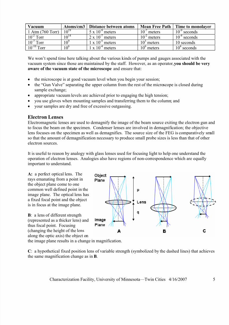
acuum Atoms/cm3 Distance between atoms Mean Free Path Time to monolayer V
1 Atm (760 Torr) 1019
5 x 10⁻⁹
meters 10-7
meters 10-9
seconds
10-2
Torr 1014
2 x 10⁻⁷
meters 10-2
meters 10-4
seconds
10-7
Torr 109
1 x 10⁻⁵
meters 103 meters 10 seconds
10-10
Torr 106
1 x 10⁻⁴
meters 106 meters 10
4 seconds
We won’t spend time here talking about the various kinds of pumps and gauges associated with they
the microscope is at good vacuum level when you begin your session;
scope is closed during
• levels are achieved prior to engaging the high tension;
; and
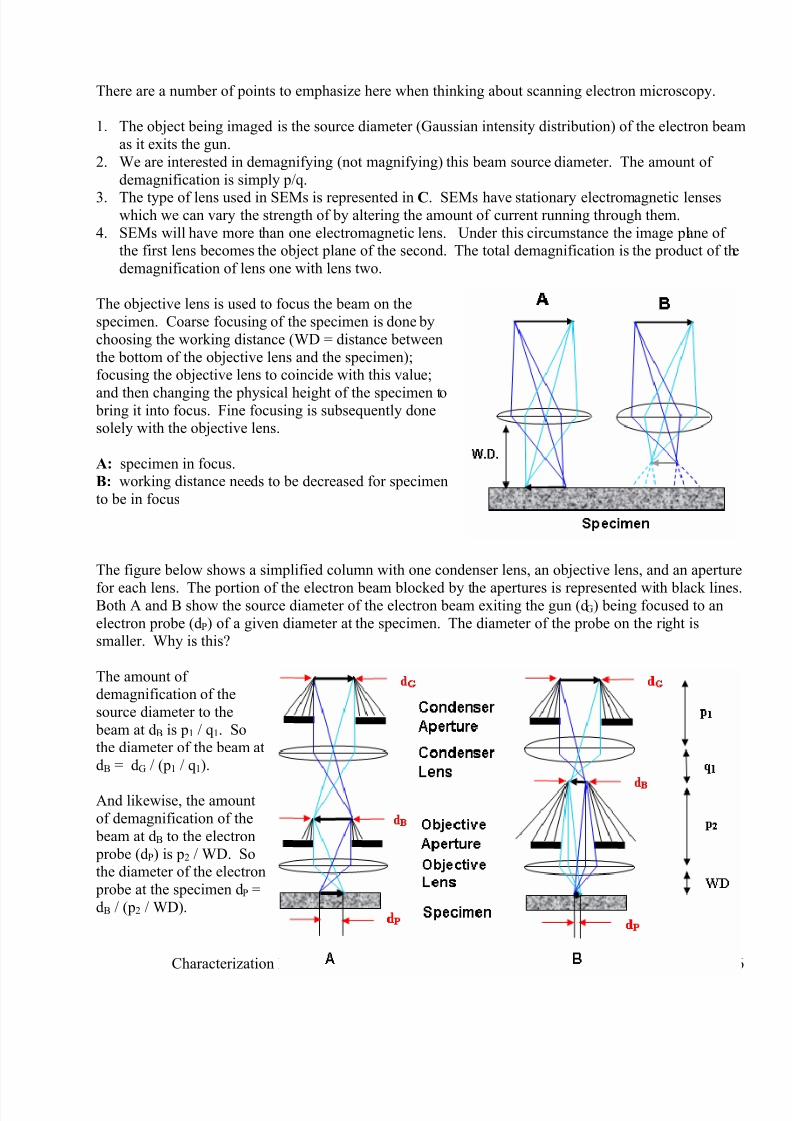
lectron Lenseses are used to demagnify the image of the beam source exiting the electron gun and
all
is useful to reason by analogy with glass lenses used for focusing light to help one understand the
: a perfect optical lens. The
the
: a lens of different strength
nd
lensn
: a hypothetical fixed position lens of variable strength (symbolized by the dashed lines) that achieves
vacuum system since those are maintained by the staff. However, as an operator, you should be ver
aware of the vacuum state of the microscope and ensure that:
•
• the “Gun Valve” separating the upper column from the rest of the microsample exchange;
appropriate vacuum
• you use gloves when mounting samples and transferring them to the column
• your samples are dry and free of excessive outgassing.
EElectromagnetic lens
to focus the beam on the specimen. Condenser lenses are involved in demagnification; the objective
lens focuses on the specimen as well as demagnifies. The source size of the FEG is comparatively smso that the amount of demagnification necessary to produce small probe sizes is less than that of other
electron sources.
Itoperation of electron lenses. Analogies also have regions of non-correspondence which are equally
important to understand.
A
rays emanating from a point inthe object plane come to one
common well defined point in
image plane. The optical lens hasa fixed focal point and the object
is in focus at the image plane.
B
(represented as a thicker lens) a
thus focal point. Focusing
(changing the height of thealong the optic axis) the object o
the image plane results in a change
in magnification.
C
the same magnification change as in B.
7/22/2019 Sem short note 1
http://slidepdf.com/reader/full/sem-short-note-1 6/29
Characterization Fac
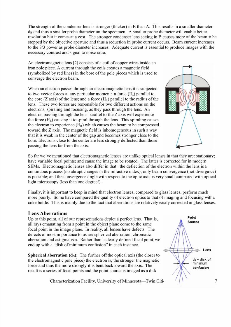
here are a number of points to emphasize here when thinking about scanning electron microscopy.
The object being imaged is the source diameter (Gaussian intensity distribution) of the electron beam
2. demagnifying (not magnifying) this beam source diameter. The amount of
3. represented in C. SEMs have stationary electromagnetic lenses
4. ane ofe
he objective lens is used to focus the beam on the
by
e;
o
: specimen in focus.ds to be decreased for specimen
he figure below shows a simplified column with one condenser lens, an objective lens, and an aperture
he amount ofof the
oat
nd likewise, the amount
T
1.
as it exits the gun.
We are interested in
demagnification is simply p/q.
The type of lens used in SEMs iswhich we can vary the strength of by altering the amount of current running through them.
SEMs will have more than one electromagnetic lens. Under this circumstance the image plthe first lens becomes the object plane of the second. The total demagnification is the product of th
demagnification of lens one with lens two.
T
specimen. Coarse focusing of the specimen is done
choosing the working distance (WD = distance between
the bottom of the objective lens and the specimen);focusing the objective lens to coincide with this valu
and then changing the physical height of the specimen t bring it into focus. Fine focusing is subsequently donesolely with the objective lens.
A
B: working distance nee
to be in focus
T
for each lens. The portion of the electron beam blocked by the apertures is represented with black lines.Both A and B show the source diameter of the electron beam exiting the gun (dG) being focused to an
electron probe (dP) of a given diameter at the specimen. The diameter of the probe on the right issmaller. Why is this?
T
ility, University of Minnesota—Twin Cities 4/16/2007 6
demagnification
source diameter to the
beam at dB is p1 / q1. Sthe diameter of the beam
dB = dG / (p1 / q1).
A
of demagnification of the
beam at dB to the electron
probe (dP) is p2 / WD. Sothe diameter of the electron
probe at the specimen dP =
dB / (p2 / WD).
7/22/2019 Sem short note 1
http://slidepdf.com/reader/full/sem-short-note-1 7/29
Characterization Facility, University of Minnesota—Twin Cities 4/16/2007
he strength of the condenser lens is stronger (thicker) in B than A. This results in a smaller diameter
o be
n electromagnetic lens [2] consists of a coil of copper wires inside an
to
hen an electron passes through an electromagnetic lens it is subjected
e
es
o far we’ve mentioned that electromagnetic lenses are unlike optical lens
nce)
inally, it is important to keep in mind that electron lenses, compared to glass lenses, perform much
a
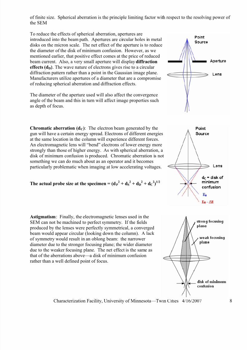
ens Aberrationsur representations depict a perfect lens. That is,
, we
pherical aberration (dS): The further off the optical axis (the closer to
k
T
dB and thus a smaller probe diameter on the specimen. A smaller probe diameter will enable betterresolution but it comes at a cost. The stronger condenser lens setting in B causes more of the beam t
stopped by the objective aperture and thus a reduction in probe current occurs. Beam current increases
to the 8/3 power as probe diameter increases. Adequate current is essential to produce images with the
necessary contrast and signal to noise ratio.
A
iron pole piece. A current through the coils creates a magnetic field(symbolized by red lines) in the bore of the pole pieces which is used
converge the electron beam.
W
to two vector forces at any particular moment: a force (HZ) parallel to
the core (Z axis) of the lens; and a force (HR ) parallel to the radius of th
lens. These two forces are responsible for two different actions on theelectrons, spiraling and focusing, as they pass through the lens. An
electron passing through the lens parallel to the Z axis will experiencthe force (HZ) causing it to spiral through the lens. This spiraling causethe electron to experience (HR ) which causes the beam to be compressed
toward the Z axis. The magnetic field is inhomogeneous in such a way
that it is weak in the center of the gap and becomes stronger close to the bore. Electrons close to the center are less strongly deflected than those
passing the lens far from the axis.
S es in that they are: stationary;
have variable focal points; and cause the image to be rotated. The latter is corrected for in modernSEMs. Electromagnetic lenses also differ in that: the deflection of the electron within the lens is a
continuous process (no abrupt changes in the refractive index); only beam convergence (not divergeis possible; and the convergence angle with respect to the optic axis is very small compared with optical
light microscopy (less than one degree!).
F
more poorly. Some have compared the quality of electron optics to that of imaging and focusing withcoke bottle. This is mainly due to the fact that aberrations are relatively easily corrected in glass lenses.
LUp to this point, all of oall rays emanating from a point in the object plane come to the same
focal point in the image plane. In reality, all lenses have defects. Thedefects of most importance to us are spherical aberration; chromaticaberration and astigmatism. Rather than a clearly defined focal point
end up with a “disk of minimum confusion” in each instance.
S
7
the electromagnetic pole piece) the electron is, the stronger the magneticforce and thus the more strongly it is bent back toward the axis. The
result is a series of focal points and the point source is imaged as a dis
7/22/2019 Sem short note 1
http://slidepdf.com/reader/full/sem-short-note-1 8/29
of finite size. Spherical aberration is the principle limiting factor with respect to the resolving power ofthe SEM
To reduce the effects of spherical aberration, apertures areintroduced into the beam path. Apertures are circular holes in metal
disks on the micron scale. The net effect of the aperture is to reduce
the diameter of the disk of minimum confusion. However, as we
mentioned earlier, that positive effect comes at the price of reduced
beam current. Also, a very small aperture will display diffractioneffects (dD). The wave nature of electrons gives rise to a circular
diffraction pattern rather than a point in the Gaussian image plane.Manufacturers utilize apertures of a diameter that are a compromise
of reducing spherical aberration and diffraction effects.
The diameter of the aperture used will also affect the convergence
angle of the beam and this in turn will affect image properties such
as depth of focus.
Chromatic aberration (dC): The electron beam generated by thegun will have a certain energy spread. Electrons of different energies
at the same location in the column will experience different forces.
An electromagnetic lens will “bend” electrons of lower energy morestrongly than those of higher energy. As with spherical aberration, a
disk of minimum confusion is produced. Chromatic aberration is notsomething we can do much about as an operator and it becomes
particularly problematic when imaging at low accelerating voltages.
Characterization Facility, University of Minnesota—Twin Cities 4/16/2007 8
The actual probe size at the specimen = (dPP
2
+ dS2
+ dD2
+ dC2
)1/2
Astigmatism: Finally, the electromagnetic lenses used in the
SEM can not be machined to perfect symmetry. If the fields
produced by the lenses were perfectly symmetrical, a converged beam would appear circular (looking down the column). A lack
of symmetry would result in an oblong beam: the narrower
diameter due to the stronger focusing plane; the wider diameterdue to the weaker focusing plane. The net effect is the same as
that of the aberrations above—a disk of minimum confusion
rather than a well defined point of focus.
7/22/2019 Sem short note 1
http://slidepdf.com/reader/full/sem-short-note-1 9/29
Operator ControlWe can begin to talk about the column parameters you can control and what effects altering them will
have. A more complete understanding will derive from our subsequent discussion of specimen-beam
interactions.
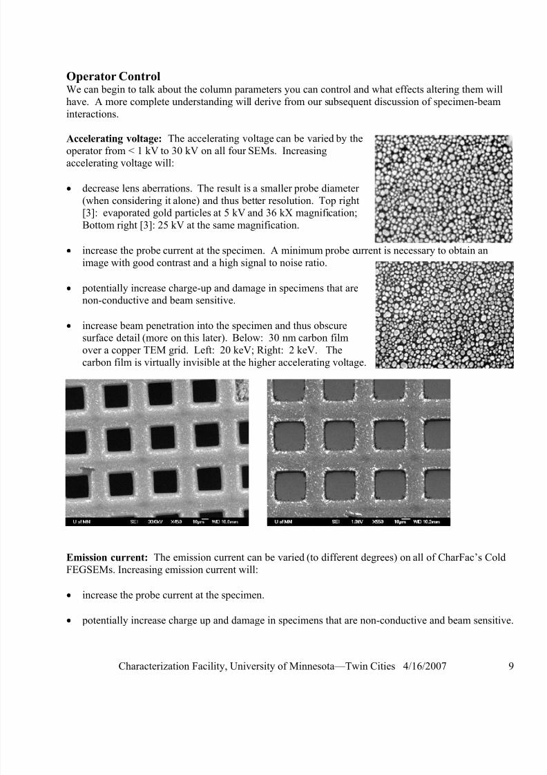
Accelerating voltage: The accelerating voltage can be varied by theoperator from < 1 kV to 30 kV on all four SEMs. Increasingaccelerating voltage will:
• decrease lens aberrations. The result is a smaller probe diameter
(when considering it alone) and thus better resolution. Top right[3]: evaporated gold particles at 5 kV and 36 kX magnification;
Bottom right [3]: 25 kV at the same magnification.
Characterization Facility, University of Minnesota—Twin Cities 4/16/2007 9
urrent is necessary to obtain an
potentially increase charge-up and damage in specimens that are
increase beam penetration into the specimen and thus obscure
tage.
• increase the probe current at the specimen. A minimum probe c
image with good contrast and a high signal to noise ratio.
•
non-conductive and beam sensitive.
•
surface detail (more on this later). Below: 30 nm carbon film
over a copper TEM grid. Left: 20 keV; Right: 2 keV. The
carbon film is virtually invisible at the higher accelerating vol
mission current: The emission current can be varied (to different degrees) on all of CharFac’s Cold
increase the probe current at the specimen.
potentially increase charge up and damage in specimens that are non-conductive and beam sensitive.
E
FEGSEMs. Increasing emission current will:
•
•
7/22/2019 Sem short note 1
http://slidepdf.com/reader/full/sem-short-note-1 10/29
Probe diameter: The probe diameter or spot size can be
varied on all four FEGSEMs by altering current to a
condenser lens. I’ve redrawn an earlier diagramrepresenting the electron beam with solid colors.
Decreasing the probe diameter will:
• enable greater resolution. Resolving small specimen
features requires probe diameters of similar dimensions.
• decrease lens aberration due to a stronger lens setting.
• decrease probe current.
Bottom left [3]: ceramic imaged with a smaller spot size.
Image is sharper but also grainier in appearance due to the
lower signal to noise ratios associated with a lower beam
current. Bottom right [3]: larger probe size results in a lesssharp but smoother image in appearance.
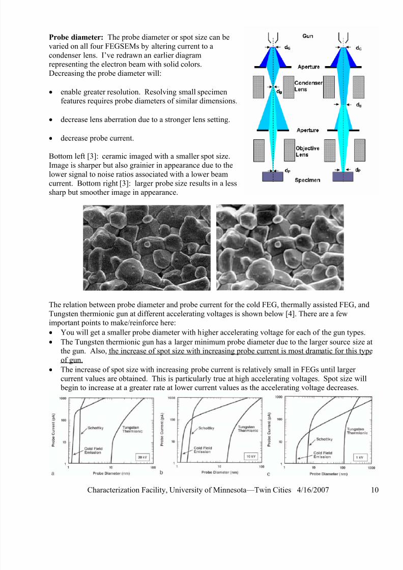
The relation between probe diameter and probe current for the cold FEG, thermally assisted FEG, and
Tungsten thermionic gun at different accelerating voltages is shown below [4]. There are a fewimportant points to make/reinforce here:
• You will get a smaller probe diameter with higher accelerating voltage for each of the gun types.
• The Tungsten thermionic gun has a larger minimum probe diameter due to the larger source size atthe gun. Also, the increase of spot size with increasing probe current is most dramatic for this type
of gun.
• The increase of spot size with increasing probe current is relatively small in FEGs until larger
current values are obtained. This is particularly true at high accelerating voltages. Spot size will begin to increase at a greater rate at lower current values as the accelerating voltage decreases.
Characterization Facility, University of Minnesota—Twin Cities 4/16/2007 10
7/22/2019 Sem short note 1
http://slidepdf.com/reader/full/sem-short-note-1 11/29
The picture element is the size of the area on the specimen from which the signal iscollected. The table below gives the linear dimension of these pixels at various
magnifications. For a given choice of magnification, images are considered to be in
sharpest focus if the signal that is measured when the beam is addressed to a given
picture element comes only from that picture element.
The probe diameter can be one of the contributing factors in determining the dimensions of
the area on the specimen from which the signal is generated. As magnification increases
and pixel dimensions decrease, overlap of adjacent pixels will eventually occur. What issurprising is that the overlap starts occurring at very low magnifications in the 5-30 kV
range. For example, a 10 keV beam with a spot size of 50 nm focused on a flat surface of Aluminumwill show overlap at 100 x magnification! Gold under the same circumstances will show overlap at
1000 x magnification! We will address the consequences of this later.
Magnification Area on Sample
(CRT screen: 10 x 10 cm)
Edge Dimension of Picture Element
(1000 x 1000 pixel scan)
10 1 cm2 10 um
100 1 mm2 1 um
1,000 100 um2 100 nm
10,000 10 um2 10 nm100,000 1 um2 1 nm
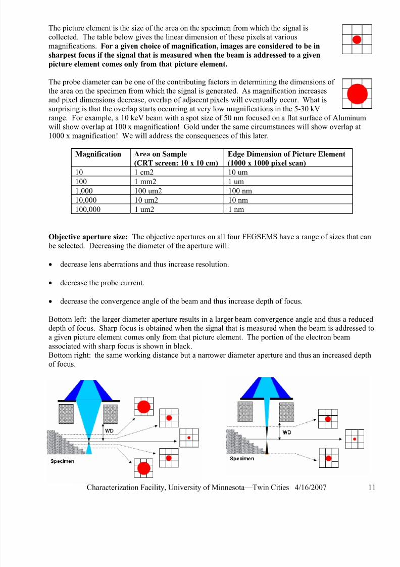
Objective aperture size: The objective apertures on all four FEGSEMS have a range of sizes that can
be selected. Decreasing the diameter of the aperture will:
• decrease lens aberrations and thus increase resolution.
• decrease the probe current.
• decrease the convergence angle of the beam and thus increase depth of focus.
Bottom left: the larger diameter aperture results in a larger beam convergence angle and thus a reduceddepth of focus. Sharp focus is obtained when the signal that is measured when the beam is addressed to
a given picture element comes only from that picture element. The portion of the electron beam
associated with sharp focus is shown in black.Bottom right: the same working distance but a narrower diameter aperture and thus an increased depth
of focus.
Characterization Facility, University of Minnesota—Twin Cities 4/16/2007 11
7/22/2019 Sem short note 1
http://slidepdf.com/reader/full/sem-short-note-1 12/29
Characterization Facility, University of Minnesota—Twin Cities 4/16/2007 12
We mentioned earlier that manufacturers utilize apertures of a diameter that are a compromise ofreducing spherical aberration and diffraction effects. Thus for the most part as an operator you will not
be altering the size of the column apertures (there will be exceptions). But there is another way to
increase depth of focus….working distance.
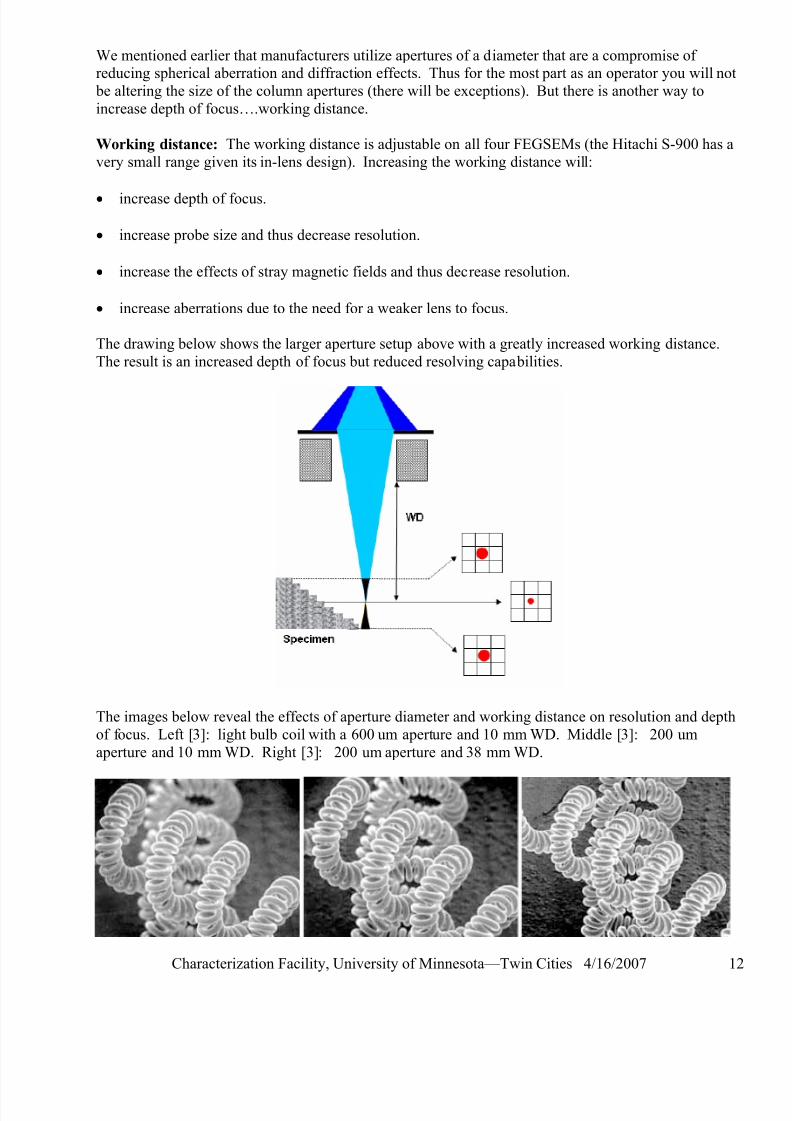
Working distance: The working distance is adjustable on all four FEGSEMs (the Hitachi S-900 has a
very small range given its in-lens design). Increasing the working distance will:
• increase depth of focus.
• increase probe size and thus decrease resolution.
increase the effects of stray magnetic fields and thus decrease resolution.
increase aberrations due to the need for a weaker lens to focus.
he drawing below shows the larger aperture setup above with a greatly increased working distance.
he result is an increased depth of focus but reduced resolving capabilities.
•
• T
T
The images below reveal the effects of aperture diameter and working distance on resolution and depth
of focus. Left [3]: light bulb coil with a 600 um aperture and 10 mm WD. Middle [3]: 200 um
aperture and 10 mm WD. Right [3]: 200 um aperture and 38 mm WD.
7/22/2019 Sem short note 1
http://slidepdf.com/reader/full/sem-short-note-1 13/29
Characterization Facility,
Focus and alignment: An important aspect of aligning the microscope is ensuring that the apertures are centered with respect
to the beam and thus the optical axis of the microscope. If an objective aperture is not centered the
image will move when you try to focus it. The way to correct this is to wobble the current to theobjective lens and align the aperture to minimize movement in both the X and Y plane. This correction
is done at successively higher magnifications—course to fine adjustment.
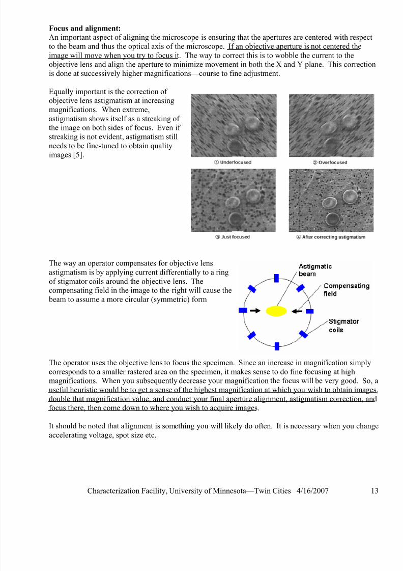
Equally important is the correction of
objective lens astigmatism at increasingmagnifications. When extreme,
astigmatism shows itself as a streaking ofthe image on both sides of focus. Even if
streaking is not evident, astigmatism still
needs to be fine-tuned to obtain qualityimages [5].
The way an operator compensates for objective lens
astigmatism is by applying current differentially to a ring
of stigmator coils around the objective lens. Thecompensating field in the image to the right will cause the
beam to assume a more circular (symmetric) form
he operator uses the objective lens to focus the specimen. Since an increase in magnification simply
n the specimen, it makes sense to do fine focusing at highdecrease your magnification the focus will be very good. So, a
sense of the highest magnification at which you wish to obtain images,
T
corresponds to a smaller rastered area omagnifications. When you subsequently
useful heuristic would be to get a
double that magnification value, and conduct your final aperture alignment, astigmatism correction, andfocus there, then come down to where you wish to acquire images.
ething you will likely do often. It is necessary when you change
voltage, spot size etc.
It should be noted that alignment is som
accelerating
University of Minnesota—Twin Cities 4/16/2007 13
7/22/2019 Sem short note 1
http://slidepdf.com/reader/full/sem-short-note-1 14/29
Characterization Facility, University of Minnesota—Twin Cities 4/16/2007 14
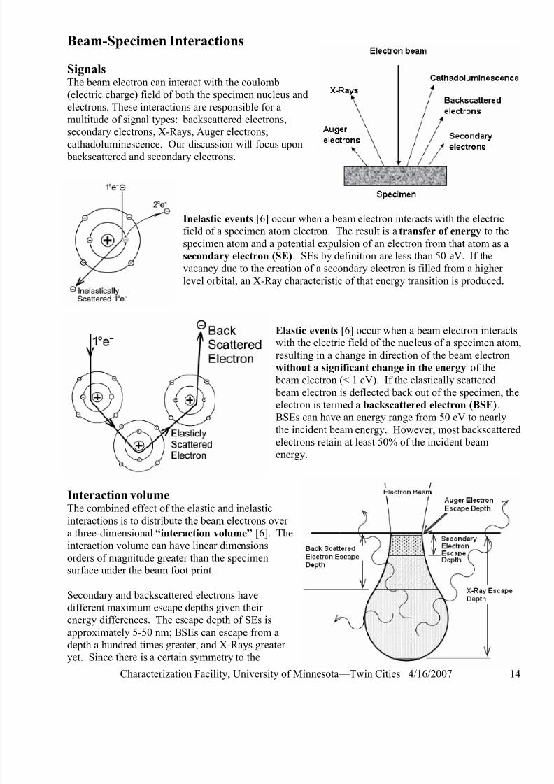
eam-Specimen Interactions
ignalshe beam electron can interact with the coulomblectric charge) field of both the specimen nucleus and
Inelastic events [6] occur when a beam
field of a specime
resulting in a change in direction of the beam electron
without a significant change in the energy of the
beam electron (< 1 eV). If the elastically scattered
beam electron is deflected back out of the specimen, theelectron is termed a backscattered electron (BSE).
BSEs can have an energy range from 50 eV to nearly
the incident beam
energy.
nsionsrders of magnitude greater than the specimensurface under the beam foot print.
Secondary and backscattered electrons havedifferent maximum escape
energy differences. The es
approximately 5-50 nm; B
depth a hundred times greayet. Since there is a certain symmetry to the
B
ST(e
electrons. These interactions are responsible for a
multitude of signal types: backscattered electrons,
secondary electrons, X-Rays, Auger electrons,cathadoluminescence. Our discussion will focus upon
backscattered and secondary electrons.
electron interacts with the electric
n atom electron. The result is a transfer of energy to the
specimen atom and a potential expulsion of an electron from that atom as a
secondary electron (SE). SEs by definition are less than 50 eV. If the
vacancy due to the creation of a secondary electron is filled from a higher
level orbital, an X-Ray characteristic of that energy transition is produced.
Elastic events [6] occur when a beam electron interactswith the electric field of the nucleus of a specimen atom
energy. However, most backscatteredelectrons retain at least 50% of the incident beam
Interaction volume
The combined effect of the elastic and inelastic
interactions is to distribute the beam electrons overa three-dimensional “interaction volume” [6]. The
interaction volume can have linear dimeo
depths given their
cape depth of SEs is
SEs can escape from a
ter, and X-Rays greater
7/22/2019 Sem short note 1
http://slidepdf.com/reader/full/sem-short-note-1 15/29
Characterization Facility, University of Minnesota—Twin Cities 4/16/2007 15
h thens.
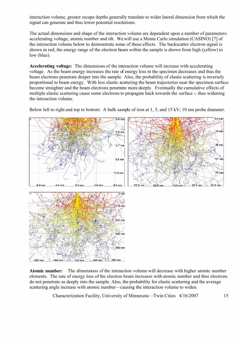
he actual dimensions and shape of the interaction volume are dependent upon a number of parameters:will use a Monte Carlo simulation (CASINO) [7] of
the interaction volume below to demonstrate som
shown in red; the energy range of the electron b
low (blue).
Accelerating voltage: The dimensions of the in
voltage. As the beam energy increases the rate o beam electrons penetrate deeper into the sample
proportional to beam energy. With less elastic s ce
become straighter and the beam electrons penetr effects ofmultiple elastic scattering cause some electrons ning
the interaction volume.
Below left to right and top to bottom: A bulk samp
interaction volume, greater escape depths generally translate to wider lateral dimension from whicsignal can generate and thus lower potential resolutio
Taccelerating voltage, atomic number and tilt. We
e of these effects. The backscatter electron signal is
eam within the sample is shown from high (yellow) to
teraction volume will increase with accelerating
f energy loss in the specimen decreases and thus the. Also, the probability of elastic scattering is inversely
cattering the beam trajectories near the specimen surfa
ate more deeply. Eventually the cumulativeto propagate back towards the surface -- thus wide
le of iron at 1, 5, and 15 kV; 10 nm probe diameter.
Atomic number: The dimensions of the interaction volume will decrease with higher atomic number
elements. The rate of energy loss of the electron beam increases with atomic number and thus electrons
do not penetrate as deep
ly into the sample. Also, the probability for elastic scattering and the averageattering angle increase with atomic number—causing the interaction volume to widen.sc
7/22/2019 Sem short note 1
http://slidepdf.com/reader/full/sem-short-note-1 16/29
Characterization Facility, University of Minnesota—Twin Cities 4/16/2007 16
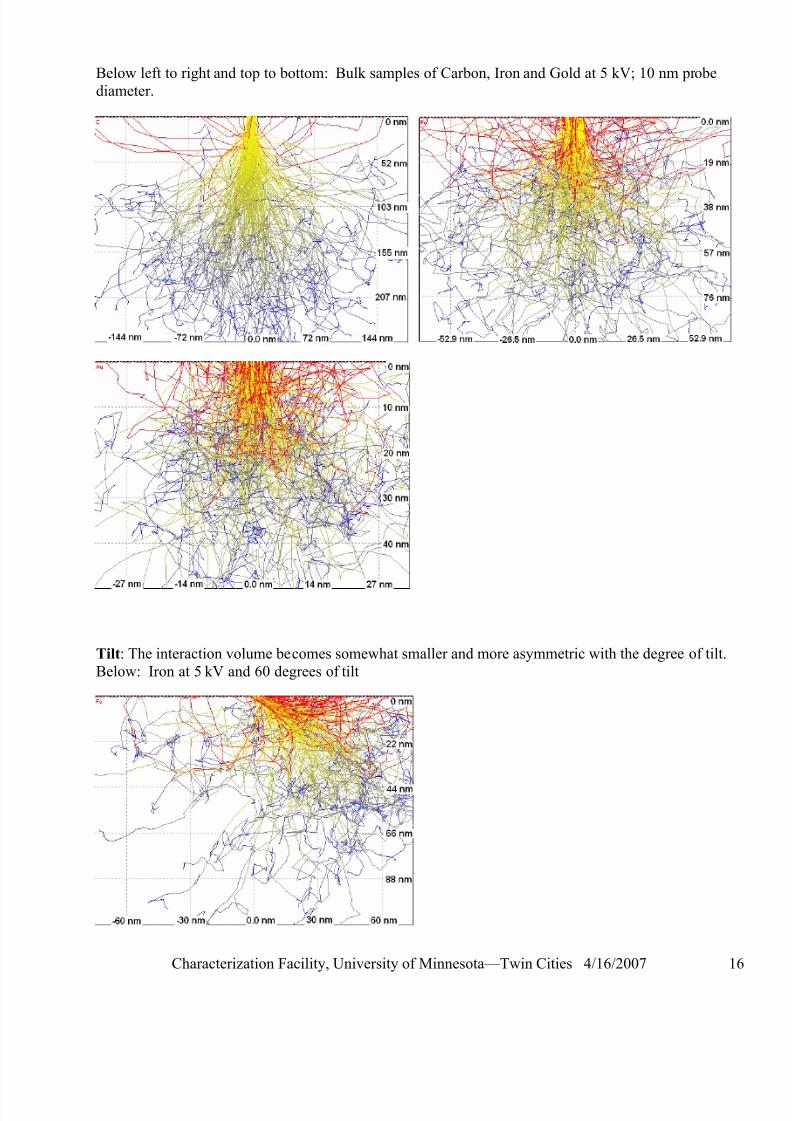
elow left to right and top to bottom: Bulk samples of Carbon, Iron and Gold at 5 kV; 10 nm probe
diameter.
B
Tilt: The interaction volume becomes somewhat smaller and more asymmetric with the degree of tilt.
Below: Iron at 5 kV and 60 degrees of tilt
7/22/2019 Sem short note 1
http://slidepdf.com/reader/full/sem-short-note-1 17/29
Characterization Facility, University of Minnesota—Twin Cities 4/16/2007 17
ackscatter electron signal
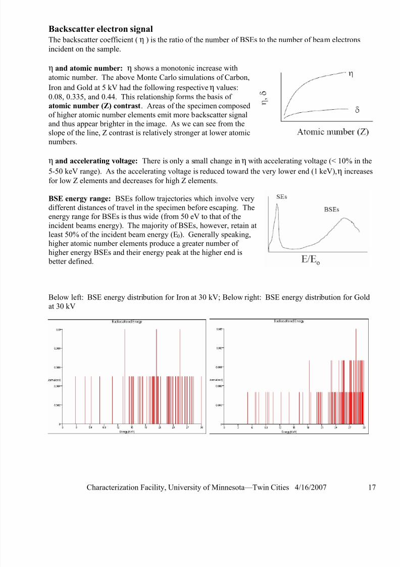
The backscatter coefficient ( η ) is the ratio of the number of BSEs to the number of beam electrons
incident on the sample.
η and atomic number: η shows a monotonic increase with
atomic number. The above Monte Carlo simulations of Carbon,
Iron and Gold at 5 kV had the following respective η values:
0.08, 0.335, and 0.44. This relationship forms the basis ofatomic number (Z) contrast. Areas of the specimen composed
of higher atomic number elements emit more backscatter signaland thus appear brighter in the image. As we can see from the
slope of the line, Z contrast is relatively stronger at lower atomic
numbers.
and accelerating voltage: There is only a small change in η with accelerating voltage (< 10% in the
-50 keV range). As the accelerating voltage is reduced toward the very lower end (1 keV), η increases
SE energy range: BSEs follow trajectories which involve verydifferent distances of travel in the specimen before escaping. Theenergy range for BSEs is thus wide (from 50 eV to that of the
incident beams energy). The majority of BSEs, however, retain at
least 50% of the incident beam energy (E0). Generally speaking,higher atomic number elements produce a greater number of
higher energy BSEs and their energy peak at the higher end is better defined.
Below left: BSE energy distribution for Iron at 30 kV; Below right: BSE energy distribution for Goldat 30 kV
B
η
5
for low Z elements and decreases for high Z elements.
B
7/22/2019 Sem short note 1
http://slidepdf.com/reader/full/sem-short-note-1 18/29
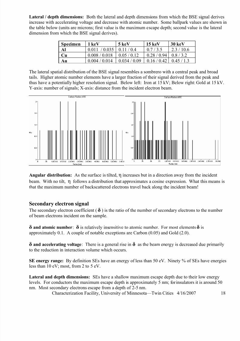
Lateral / depth dimensions: Both the lateral and depth dimensions from which the BSE signal derivesincrease with accelerating voltage and decrease with atomic number. Some ballpark values are shown in
the table below (units are microns; first value is the maximum escape depth; second value is the lateral
imension from which the BSE signal derives).d
Characterization Facility, University of Minnesota—Twin Cities 4/16/2007 18
e
Specimen 1 keV 5 keV 15 k V 30 keV
Al 0.011 / 0.035 0.11 / 0.4 0.7 / 3.5 2.3 / 10.6
Cu 0.008 / 0.018 0.05 / 0.12 0.28 / 0.94 0.8 / 3.2
Au 0.004 / 0.014 0.034 / 0.09 0.16 / 0.42 0.45 / 1.3
The lateral spatial distribution of the BSE signal resembles a sotails. Higher at
mbrero with a central peak and broadomic number elements have a larger fraction of their signal derived from the peak and
us have a potentially higher resolution signal. Below left: Iron at 15 kV; Below right: Gold at 15 kV.
-axis: number of signals; X-axis: distance from the incident electron beam.
th
Y
Angular distribution: As the surface is tilted, η increases but in a direction away from the incident
. With no tilt, η follows a distribution that approximates a cosine expression. What this means is
at the maximum number of backscattered electrons travel back along the incident beam!
econdary electron signal
proximately 0.1. A couple of notable exceptions are Carbon (0.05) and Gold (2.0).
δ and accelerating voltage: T s th erg sed due primarily
to the reduction i eraction v c
E energy range: By definition SEs have an energy of less than 50 eV. Ninety % of SEs have energies
insulators it is around 50nm. Most secondary electrons escape from a depth of 2-5 nm.
beam
th
S
The secondary electron coefficient ( δ ) is the ratio of the number of secondary electrons to the number
of beam electrons incident on the sample.
δ and atomic number: δ is relatively insensitive to atomic number. For most elements δ is
ap
here is a general rise in δ a e beam en y is decrea
n int olume which o curs.
S
less than 10 eV; most, from 2 to 5 eV.
Lateral and depth dimensions: SEs have a shallow maximum escape depth due to their low energy
levels. For conductors the maximum escape depth is approximately 5 nm; for
7/22/2019 Sem short note 1
http://slidepdf.com/reader/full/sem-short-note-1 19/29
Characterization Facility, University of Characterization Facility, University of
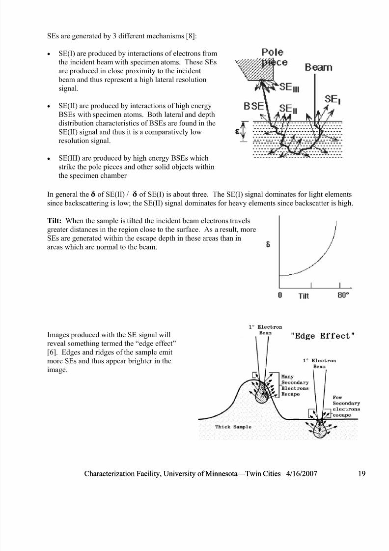
SEs are generated by 3 different mechanisms [8]:
• SE(I) are produced by interactions of electrons fromthe incident beam with specimen atoms. These SEs
are produced in close proximity to the incident
beam and thus represent a high lateral resolution
signal.
• SE(II) are produced by interactions of high energy
BSEs with specimen atoms. Both lateral and depthdistribution characteristics of BSEs are found in the
SE(II) signal and thus it is a comparatively low
resolution signal.
general the δ of SE(II) / δ of SE(I) is about three. The SE(I) signal dominates for light elementsE(II) signal dominates for heavy elements since backscatter is high.
surface. As a result, more
]. Edges and ridges of the sample emit
age.
• SE(III) are produced by high energy BSEs which
strike the pole pieces and other solid objects within
the specimen chamber
Insince backscattering is low; the S
Tilt: When the sample is tilted the incident beam electrons travelsreater distances in the region close to theg
SEs are generated within the escape depth in these areas than in
areas which are normal to the beam.
Images produced with the SE signal willreveal something termed the “edge effect”
[6
more SEs and thus appear brighter in the
im
Minnesota—Twin Cities 4/16/2007 19Minnesota—Twin Cities 4/16/2007 19
7/22/2019 Sem short note 1
http://slidepdf.com/reader/full/sem-short-note-1 20/29
Characterization Facility, University of Minnesota—Twin Cities 4/16/2007 20
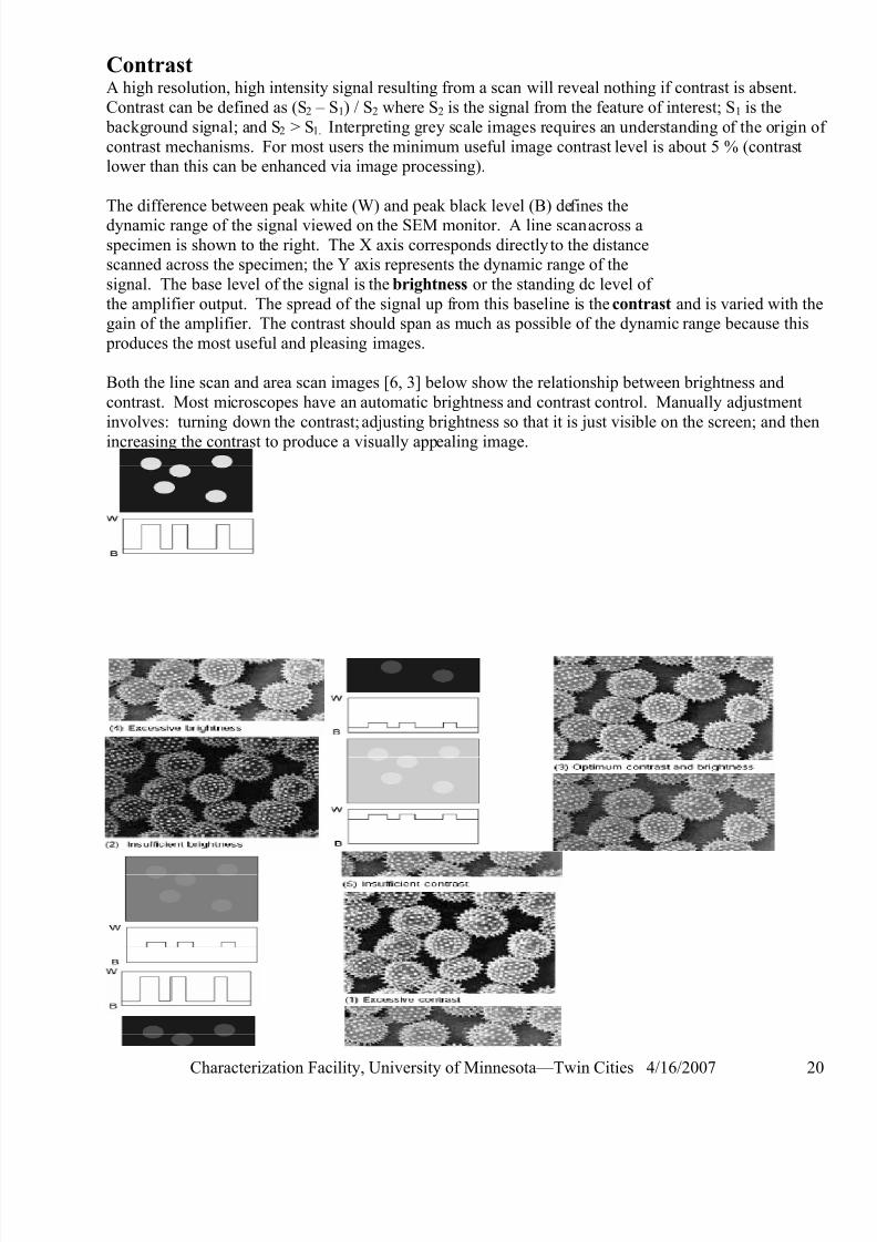
ontrast
2 – S1) / S2 where S2 is the signal from the feature of interest; S1 is the
ackground sig al; and S > S Interpreting grey scale images requires an understanding of the origin of
fin across a
to the distancexis represents the dynamic range of the
signal. The base level of the signal is the brightness or the standing dc level of
e amplifier output. The spread of the signal up from this baseline is the contrast and is varied with thegain of the amplifier. The contrast should span as much as possible of the dynamic range because this
roduces the most useful and pleasing images.
oth the line scan and area scan images [6, 3] below show the relationship between brightness and
contrast. Most microscopes have an automatic brightness and contrast control. Manually adjustment
volves: turning down the contrast;
increasing the contrast to produce a visually app
CA high resolution, high intensity signal resulting from a scan will reveal nothing if contrast is absent.
Contrast can be defined as (S
b n 2 1.
contrast mechanisms. For most users the minimum useful image contrast level is about 5 % (contrastlower than this can be enhanced via image processing).
The difference between peak white (W) and peak black level (B) dedynamic range of the signal viewed on the SEM monitor. A line scan
specimen is shown to the right. The X axis corresponds directlyscanned across the specimen; the Y a
es the
th
p
B
in adjusting brightness so that it is just visible on the screen; and then
ealing image.
7/22/2019 Sem short note 1
http://slidepdf.com/reader/full/sem-short-note-1 21/29
Characterization Facility, University of
The backscatter coefficient increases with increasing
atomic number and so higher atomic numberelements will appear brighter in the image. Elements
widely separated in atomic number will result in thegreatest contrast. For pairs of elements of similaratomic number, the contrast between them decreases
with increasing atomic number.
We mentioned earlier when discussing the angularistribution of BSEs th t a large percentage travel
. The backscatter
detectors we have at CharFac are mounted directlyunder the objective lens to take advantage of this
fact. The detectors are circular and have a hole in
the middle to allow the electron beam to passthrough.
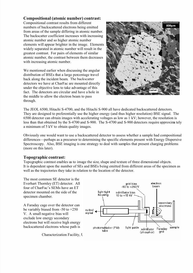
The JEOL 6500, Hitachi S-4700, and the Hitachi S-900 all have dedicated backscattered detectors.
They are designed to preferentially use the higher energy (and thus higher resolution) BSE signal. The6500 detector can obtain images with accelerating voltages as low as 1 kV; however, the resolution is
less than that obtained by the S-4700 and S-900. The S-4700 and S-900 detectors require approxim tely
a minimum of 5 kV to obtain quality images.
Obviously one would want to use a backscattered detector to assess whether a sample had compositional
differences—perhaps as a precursor to determining the specific elements present with Energy Dispersive
Spectroscopy. Also, BSE imaging is one strategy to deal with samples that present charging problems(more on this later).
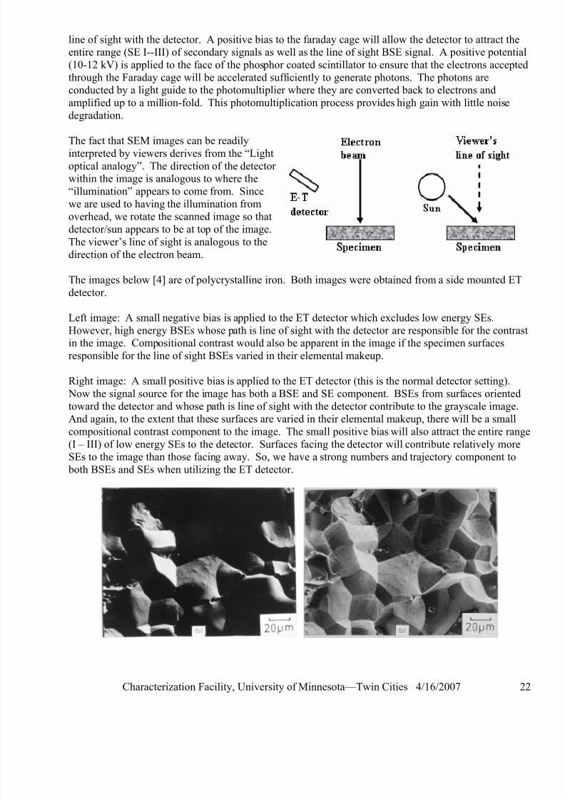
Topographic contrast:opographic contrast enables u image the size, shape and texture of three dimensional objects.
is dependent upon the number of SEs and BSEs being emitted from different areas of the specimen astion of the detector.
xclude low energy secondary
Compositional (atomic number) contrast:Compositional contrast results from different
numbers of backscattered electrons being emittedfrom areas of the sample differing in atomic number.
d
back along the incident beam
a
a
T s to
Itwell as the trajectories they take in relation to the loca
The most common SE detector is theEverhart Thornley (ET) detector. All
four of CharFac’s SEMs have an ET
detector mounted on the side of thespecimen chamber.
A Faraday cage over the detector can
be variably biased from -50 to +250V. A small negative bias will
e
Minnesota—Twin Cities 4/16/2007 21
electrons but will receive high energy backscattered electrons whose path is
7/22/2019 Sem short note 1
http://slidepdf.com/reader/full/sem-short-note-1 22/29
Characterization Facility, University of
phor coated scintillator to ensure that the electrons accepted
rough the Faraday cage will be accelerated sufficiently to generate photons. The photons are
terpreted by viewers derives from the “Light
the illumination fromverhead, we rotate the scanned image so that
p of the image.
he images below [4] are of polycrystalline iron. Both images were obtained from a side mounted ET
ath is line of sight with the detector are responsible for the contrastositional contrast would also be apparent in the image if the specimen surfaces
sponsible for the line of sight BSEs varied in their elemental makeup.
applied to the ET detector (this is the normal detector setting).
mage has both a BSE and SE component. BSEs from surfaces orientedath is line of sight with the detector contribute to the grayscale image.
se surfaces are varied in their elemental makeup, there will be a smallnt to the image. The small positive bias will also attract the entire range
ctor. Surfaces facing the detector will contribute relatively moreg away. So, we have a strong numbers and trajectory component to
e ET detector.
line of sight with the detector. A positive bias to the faraday cage will allow the detector to attract theentire range (SE I--III) of secondary signals as well as the line of sight BSE signal. A positive potential
(10-12 kV) is applied to the face of the phos
thconducted by a light guide to the photomultiplier where they are converted back to electrons and
amplified up to a million-fold. This photomultiplication process provides high gain with little noise
degradation.
The fact that SEM images can be readilyin
optical analogy”. The direction of the detectorwithin the image is analogous to where the
“illumination” appears to come from. Since
we are used to havingo
detector/sun appears to be at to
The viewer’s line of sight is analogous to the
direction of the electron beam.
Tdetector.
Left image: A small negative bias is a
However, high energy BSEs whose pin the image. Comp
pplied to the ET detector which excludes low energy SEs.
re
Right image: A small positive bias is
Now the signal source for the itoward the detector and whose p
And again, to the extent that thecompositional contrast compone
(I – III) of low energy SEs to the deteSEs to the image than those facin
both BSEs and SEs when utilizing th
Minnesota—Twin Cities 4/16/2007 22
7/22/2019 Sem short note 1
http://slidepdf.com/reader/full/sem-short-note-1 23/29
Characterization Facility, University of Minnesota—Twin Cities 4/16/2007 23
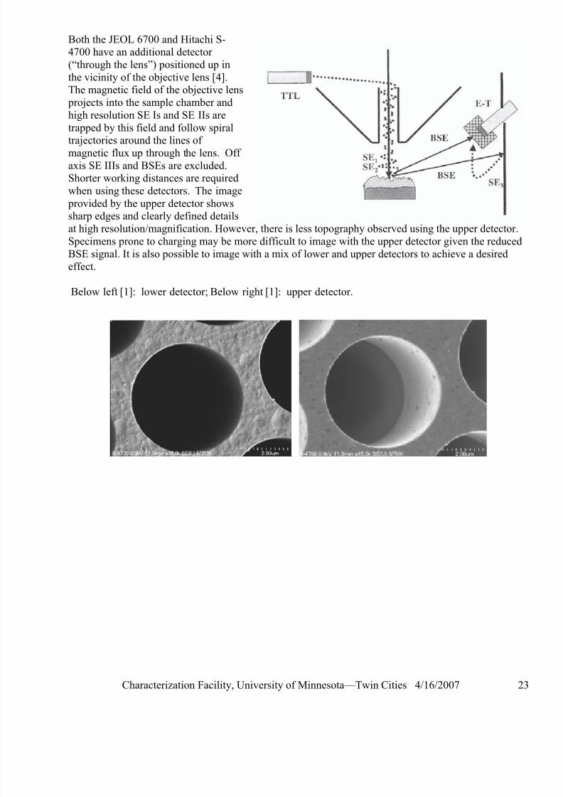
700 have an additional detector
of the objective lens [4].he magnetic field of the objective lens
agnetic flux up through the lens. Off
f lower and upper detectors to achieve a desiredfect.
Below left [1]: lower detector; Below right [1]: upper detector.
Both the JEOL 6700 and Hitachi S-4
(“through the lens”) positioned up in
the vicinityT
projects into the sample chamber and
high resolution SE Is and SE IIs are
trapped by this field and follow spiral
trajectories around the lines ofm
axis SE IIIs and BSEs are excluded.Shorter working distances are required
when using these detectors. The image
provided by the upper detector showssharp edges and clearly defined details
at high resolution/magnification. However, there is less topography observed using the upper detector.
Specimens prone to charging may be more difficult to image with the upper detector given the reduced
BSE signal. It is also possible to image with a mix oef
7/22/2019 Sem short note 1
http://slidepdf.com/reader/full/sem-short-note-1 24/29
Characterization Fac
ality images require a high signal to noise ratio. The signal intensity from multiple scans from a
istribution corresponds to
oise (N). The signal to noise ratio =
/N = n / n1/2
= n1/2
.
An observer can distinguish small
features in the presence of noise provided that the change in signalΔS is greater than the noise (N) by a factor of 5. Thus the
smallest beam current that will
permit a given contrast level (C =ΔS/S) to be discerned is:
n > (5/C)2.
perhaps more intuitive way to
ink about the relationships
etween contrast, beam current
d scan rate is the graph to theght. It is necessary to use
me combination of high beam
rrent and a slow scan speed
order to detect objects of
all size and low contrast in
SEM.
igh resolution imaging
he resolution is the minimum spacing at which two features of the specimen can be recognized asistinct or separate. In order to obtain high resolution images we need to adjust the probe diameter to
e scale of interest and ensure that a minimum level of contrast exists with the appropriate probeettings.
am, and the SE IIs that are generated from BSEs of high energy and
We also know that, even with small probe diameters, the interaction
el overlap will occur at surprisingly small magnifications.
ways to achieve high resolution [4]:
resolution signal (high resolution at high kV).
similar ranges for the “high” and “low” resolution signals (high
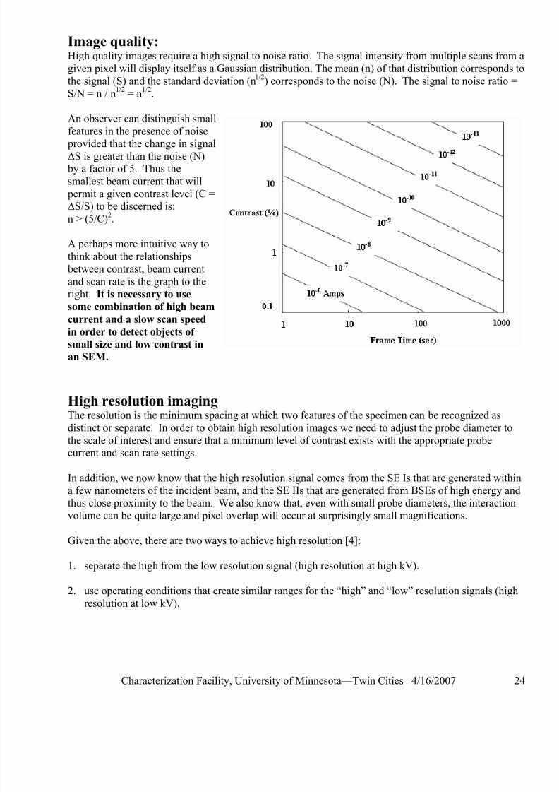
Image quality:High qu
given pixel will display itself as a Gaussian distribution. The mean (n) of that d
the signal (S) and the standard deviation (n1/2
) corresponds to the n
S
A
th
b
anri
so
cu
in
sm
an
H
Td
thcurrent and scan rate s
In addition, we now know that the high resolution signal comes from the SE Is that are generated withina few nanometers of the incident be
thus close proximity to the beam.
volume can be quite large and pix
Given the above, there are two
1. separate the high from the low
2. use operating conditions that create
resolution at low kV).
ility, University of Minnesota—Twin Cities 4/16/2007 24
7/22/2019 Sem short note 1
http://slidepdf.com/reader/full/sem-short-note-1 25/29
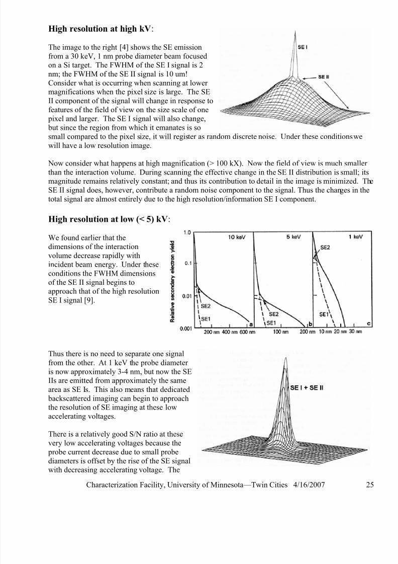
High resolution at high kV:
Characterization Facility, University of Minnesota—Twin Cities 4/16/2007 25
he image to the right [4] shows the SE emission
onsider what is occurring when scanning at loweragnifications when the pixel size is large. The SE
ge in response to
we
.
e
ges in the
SE I component.
dim n
olume decrease rapidly withcident beam energy. Under these
onditions the FWHM dimensions
f the SE II signal begins to pproach that of the high resolution
T
from a 30 keV, 1 nm probe diameter beam focusedon a Si target. The FWHM of the SE I signal is 2
nm; the FWHM of the SE II signal is 10 um!
Cm
II component of the signal will chanfeatures of the field of view on the size scale of one pixel and larger. The SE I signal will also change,
but since the region from which it emanates is so
small compared to the pixel size, it will register as random discrete noise. Under these conditions
ill have a low resolution imagew
Now consider what happens at high magnification (> 100 kX). Now the field of view is much smaller
than the interaction volume. During scanning the effective change in the SE II distribution is small; itsmagnitude remains relatively constant; and thus its contribution to detail in the image is minimized. Th
E II signal does, however, contribute a random noise component to the signal. Thus the chanS
total signal are almost entirely due to the high resolution/information
High resolution at low (< 5) kV:
We found earlier that theensions of the interactio
vin
c
oa
SE I signal [9].
Thus there is no need to separate one signal
from the other. At 1 keV the probe diameter
is now approximately 3-4 nm, but now the SEIIs are emitted from approximately the same
area as SE Is. This also means that dedicated
backscattered imaging can begin to approachthe resolution of SE imaging at these low
accelerating voltages.
There is a relatively good S/N ratio at these
very low accelerating voltages because the
probe current decrease due to small probe
diameters is offset by the rise of the SE signalwith decreasing accelerating voltage. The
7/22/2019 Sem short note 1
http://slidepdf.com/reader/full/sem-short-note-1 26/29
Characterization Facility, University of Minnesota—Twin Cities 4/16/2007 26
ownside of low kV imaging is that the performance of the optical system is decreased due to aneam is more susceptible to stray magnetic fields.
can bemination results from the
with residual gases and
e. SE imaging in particular
their low energy level.
ens;
decreasing the probe current;
avoiding high magnification except where essential;
aligning the microscope on areas of the specimen not used for imaging;
using a cold finger (anticontamination trap) in the column if available.
lo
E yield
eld can ben
. Coatingshicker
pproximate the escape depth for
Es and thus produce a high SE yield. However, the
apparent inaging will
of the range
he thinfeatures.
hange in metal thickness that occurs as the beam is
hargingterial cannot effectively conduct the beam energy imparted to it. A
n the specimen as the beam electrons lose all of their initial
e cimen. This charge flows to ground if the specimen is a conductorken, even a conducting specimen quickly
ting specimens will obviously
acc . The ensuing image will “glow” or cause streaks or general distortion in the image asc deflected.
oth conducting and non-conducting samples are attached to their holders with conductive tapes or
paints. Non-conducting samples are also coated with thin conductive films (Carbon, Gold-Palladium,Platinum etc) to facilitate electron flow.
dincrease in chromatic aberration and the b
In addition, contaminationvoltage microscopy [3]. Conta
interaction of the electron beam
hydrocarbons on the specimen surfac
is vulnerable to contamination given
Contamination can be reduced by:
• ensuring the cleanliness of specim
a serious limitation to low
• •
•
•
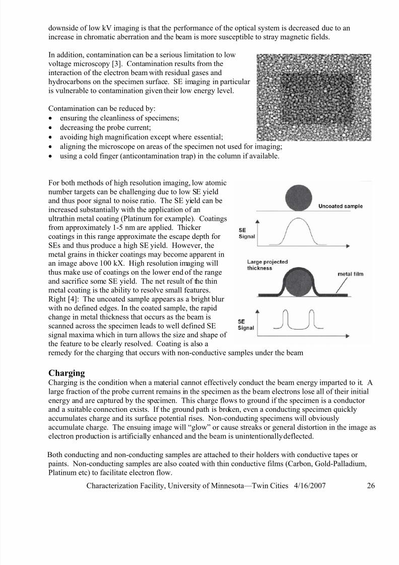
For both methods of high resolution imaging,
number targets can be challenging due to low S
and thus poor signal to noise ratio. The SE yiincreased substantially with the application of a
ultrathin metal coating (Platinum for example)from approximately 1-5 nm are applied. T
coatings in this range a
w atomic
S
metal grains in thicker coatings may becomean image above 100 kX. High resolution im
thus make use of coatings on the lower end
and sacrifice some SE yield. The net result of tmetal coating is the ability to resolve small
Right [4]: The uncoated sample appears as a bright blurwith no defined edges. In the coated sample, the rapidc
scanned across the specimen leads to well defined SE
signal maxima which in turn allows the size and shape ofthe feature to be clearly resolved. Coating is also a
remedy for the charging that occurs with non-conductive samples under the beam
CCharging is the condition when a ma
large fraction of the probe current remains i
en rgy and are captured by the speand a suitable connection exists. If the ground path is bro
accumulates charge and its surface potential rises. Non-conduc
umulate chargeele tron production is artificially enhanced and the beam is unintentionally
B
7/22/2019 Sem short note 1
http://slidepdf.com/reader/full/sem-short-note-1 27/29
Characterization Facility, University of Minnesota—Twin Cities 4/16/2007 27
pe
the selected area.
le.
on going to the lower magnification), negative
ltage.
pears, positive charging is probable. Therefore, raisentamination is most likely the problem.
s, so be sure to check these conditionstend to use.
llowing strategies can be used to reduce
the amount of incident electrons and the
me integration;
2 value for insulators.
e. This positive form
rimary electron beam provides. Rather than glowing, a dark box (from the scan footprint) wille charging are voltages at which
e sample achieves charge balance: E1 and E2. For each material, E1 and E2 are constants. E2 is the
is found at a higher accelerating voltage, thus utilizing a
Scan-square method of testing the conductivity of a s
1. Focus on an area at a high magnification.2. Wait a few seconds, letting the beam irradiate
3. Reduce the magnification and observe the samp
4. If a bright square appears (which may disappear up
charging is probable. Therefore, lower the vo
5. If a dark square appears, and then quickly disapthe voltage. Note: If the dark square remains, co
6. The effect of charging is exacerbated at higher magnificationat levels near to or at the highest magnification you in
In addition to the application of thin metal coatings, the fo
charging:
• reducing the probe current;
• lowering the accelerating voltage;
• tilting the specimen to find a balanced point betweenamount of electrons that go out of the specimen;
• imaging with BSEs;
cimen [1]:
• use rapid scan rates and fra
• find the E
E2 Value [1]: When the
sum of the BSE and SEcoefficient is measured at
very low kV, it is found that
there is an energy rangeover which this sum is
positiv
of charging results frommore electrons being
emitted from the sample
than the pappear as secondary electrons are emitted. Flanking this area of positiv
th
value to seek for uncoated observation since it
higher resolution condition of the SEM.
7/22/2019 Sem short note 1
http://slidepdf.com/reader/full/sem-short-note-1 28/29
Characterization Facility, University of Minnesota—Twin Cities 4/16/2007 28
Ma
terial E2 (kV)
Ka ton 0.4 p
Electron resist 0.55—0.7
Ny on 1.18l
5% PB7/nylon 1.40
Acetal 1.65
Polyvinyl chloride 1.65
Teflon 1.82
Glass passivation 2.0
GaAs 2.6
Quartz 3.0
Alumina 4.2
Specimen damage by electron beamThe loss of electron beam energy in the specimen occurs mostly in the form of heat generation at the
irradiated point. Polymer materials and biological specimens, which are generally not resistant to heat,
are easily damaged by the electron beam, because of their low heat conductivity.
The following strategies can be used to avoid this damage:
decrease the electron beam intensity;
shorten the exposure time, even though this reduces image smoothness slightly;
image large scanning areas with low magnifications;
control the thickness of coating metal on the specimen surface. It is also advisable to adjust beforehand the astigmatism and brightness using another field of view and then image the actual
field as quickly as possible.
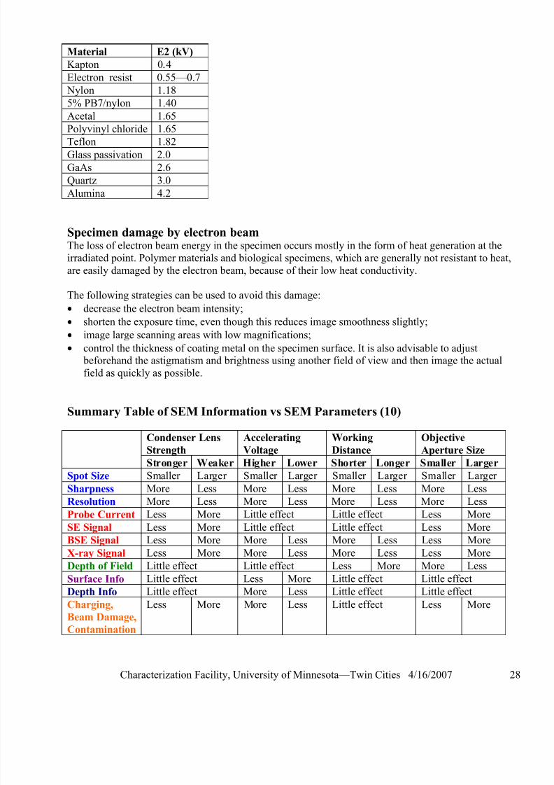
ummary Table of SEM Information vs SEM Parameters (10)
Condenser Lens
Strength
Accelerating
Voltage
Working
Distance
Objective
Aperture Size
•
•
•
•
S
Stronger Weaker Higher Lower Shorter Longer Smaller Larger
Spot Size Sm r Larger Smaller Larger Smaller Larger Smaller Largeralle
Sharpness M ss More Less More Less More Lessore Le
Resolution More Less More Less More Less More Less
Probe Current Le More Little effect Little effect Less Moress
SE Signal Le More Little effect Little effect Less Moress
BSE Signal Le More More Less More Less Less Moress
X-ray Signal Less More More Less More Less Less MoreDepth of Field Little effect Little effect Less More More Less
Surface Info Little effect Less More Little effect Little effect
Depth Info Little effect More Less Little effect Little effect
Charging,
eam Damage,
ontamination
Less More More Less Little effect Less More
B
C
7/22/2019 Sem short note 1
http://slidepdf.com/reader/full/sem-short-note-1 29/29
[1] FE-SEM Training Manual, Hitachi Scientific Instruments
[2] http://www.microscopy.ethz.ch/lens.htm
[3] JEOL: A Guide to Scanning Microscope Observationand X-Ray Microanalysis”.[4] Joseph Goldstein et al. “Scanning Electron Microscopy
[5] JEOL 6700 SEM User Manual
[6] http://www.cas.muohio.edu/~emfweb/EMTheory/OH_Index.html
[7] http://www.gel.usherbrooke.ca/casino/What.html
[8] http://emalwww.engin.umich.edu/courses/semlectures/semlec.html#anchor659909[9] 9
[10
David C. Joy. “Low Voltage Scanning Electron Microscopy”, Hitachi Instrument News, July 198
] JEOL training documents