S34MS16G2, 16 Gb, 4-Bit ECC, x8 I/O, and 1.8V VCC NAND ...
16
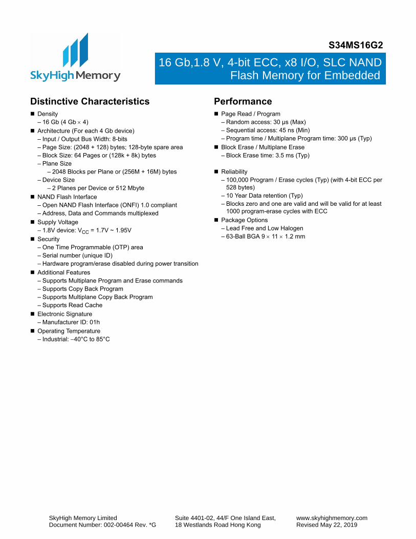
S34MS16G2 Distinctive Characteristics Density – 16 Gb (4 Gb 4) Architecture (For each 4 Gb device) – Input / Output Bus Width: 8-bits – Page Size: (2048 + 128) bytes; 128-byte spare area – Block Size: 64 Pages or (128k + 8k) bytes – Plane Size – 2048 Blocks per Plane or (256M + 16M) bytes – Device Size – 2 Planes per Device or 512 Mbyte NAND Flash Interface – Open NAND Flash Interface (ONFI) 1.0 compliant – Address, Data and Commands multiplexed Supply Voltage – 1.8V device: V CC = 1.7V ~ 1.95V Security – One Time Programmable (OTP) area – Serial number (unique ID) – Hardware program/erase disabled during power transition Additional Features – Supports Multiplane Program and Erase commands – Supports Copy Back Program – Supports Multiplane Copy Back Program – Supports Read Cache Electronic Signature – Manufacturer ID: 01h Operating Temperature – Industrial: 40°C to 85°C Performance Page Read / Program – Random access: 30 µs (Max) – Sequential access: 45 ns (Min) – Program time / Multiplane Program time: 300 µs (Typ) Block Erase / Multiplane Erase – Block Erase time: 3.5 ms (Typ) Reliability – 100,000 Program / Erase cycles (Typ) (with 4-bit ECC per 528 bytes) – 10 Year Data retention (Typ) – Blocks zero and one are valid and will be valid for at least 1000 program-erase cycles with ECC Package Options – Lead Free and Low Halogen – 63-Ball BGA 9 11 1.2 mm 16 Gb,1.8 V, 4-bit ECC, x8 I/O, SLC NAND Flash Memory for Embedded SkyHigh Memory Limited Document Number: 002-00464 Rev. *G Suite 4401-02, 44/F One Island East, 18 Westlands Road Hong Kong www.skyhighmemory.com Revised May 22, 2019
Transcript of S34MS16G2, 16 Gb, 4-Bit ECC, x8 I/O, and 1.8V VCC NAND ...
S34MS16G2
Distinctive Characteristics Density
– 16 Gb (4 Gb 4)
Architecture (For each 4 Gb device)– Input / Output Bus Width: 8-bits– Page Size: (2048 + 128) bytes; 128-byte spare area– Block Size: 64 Pages or (128k + 8k) bytes– Plane Size
– 2048 Blocks per Plane or (256M + 16M) bytes– Device Size
– 2 Planes per Device or 512 Mbyte
NAND Flash Interface– Open NAND Flash Interface (ONFI) 1.0 compliant– Address, Data and Commands multiplexed
Supply Voltage– 1.8V device: VCC = 1.7V ~ 1.95V
Security– One Time Programmable (OTP) area– Serial number (unique ID)– Hardware program/erase disabled during power transition
Additional Features– Supports Multiplane Program and Erase commands– Supports Copy Back Program– Supports Multiplane Copy Back Program– Supports Read Cache
Electronic Signature– Manufacturer ID: 01h
Operating Temperature– Industrial: 40°C to 85°C
Performance Page Read / Program
– Random access: 30 µs (Max)– Sequential access: 45 ns (Min)– Program time / Multiplane Program time: 300 µs (Typ)
Block Erase / Multiplane Erase– Block Erase time: 3.5 ms (Typ)
Reliability– 100,000 Program / Erase cycles (Typ) (with 4-bit ECC per
528 bytes)– 10 Year Data retention (Typ)– Blocks zero and one are valid and will be valid for at least
1000 program-erase cycles with ECC
Package Options– Lead Free and Low Halogen– 63-Ball BGA 9 11 1.2 mm
16 Gb,1.8 V, 4-bit ECC, x8 I/O, SLC NAND Flash Memory for Embedded
SkyHigh Memory LimitedDocument Number: 002-00464 Rev. *G
Suite 4401-02, 44/F One Island East, 18 Westlands Road Hong Kong
www.skyhighmemory.comRevised May 22, 2019

S34MS16G2
ContentsDistinctive Characteristics .................................................. 1
Performance.......................................................................... 1
1. General Description..................................................... 3
2. Connection Diagram.................................................... 3
3. Pin Description............................................................. 4
4. Block Diagrams............................................................ 5
5. Addressing ................................................................... 7
6. Read Status Enhanced ................................................ 7
7. Read ID.......................................................................... 77.1 Read Parameter Page ................................................... 9
8. Electrical Characteristics .......................................... 128.1 Valid Blocks ................................................................. 128.2 DC Characteristics ....................................................... 12
8.3 Pin Capacitance............................................................ 13Power Consumptions and Pi8.4 n Capacitance for Allowed Stacking Configurations................................................ 13
Physical Interface9. ....................................................... 1463-Ball BGA Package .........................................9.1 .......... 14
Ordering Information10. .................................................. 15
Revision History11. .......................................................... 16Document History Page ......................................................16
Document Number: 002-00464 Rev. *G
Page 2 of 16

S34MS16G2
1. General DescriptionThe SkyHigh S34MS16G2 16-Gb NAND is offered in 1.8V VCC with x8 I/O interface. This document contains information for theS34MS16G2 device, which is a quad-die stack of four S34MS04G2 die. For detailed specifications, please refer to the discrete die data sheet: S34MS01G2_04G2.
2. Connection Diagram
Figure 2.1 63-BGA Contact, x8 Device (Balls Down, Top View)
F8F7F6F5F4F3
E8E7E6E5E4E3
D8D7D6D5D4D3
C8C7C6C5C4C3
RB#WE#CE#VSSALEWP#
NCNCNCCLERE#VCC (1)
NCNCNCNCNCNC
G8G7G6G5G4G3
NCVSS (1)NCNCNCNC
H8H7H6H5H4H3
VccNCNCNCI/O0NC
B9
A9
NC
NC
A2
NC
NCNCNCNCVCC (1)NC
B10
A10
NC
NC
B1
A1
NC
NC
J8J7J6J5J4J3
I/O7I/O5VCCNCI/O1NC
K8K7K6K5K4K3
VSSI/O6I/O4I/O3I/O2VSS
L9
NC
L2
NC
L10
NC
L1
NC
M9
NC
M2
NC
M10
NC
M1
NC
Document Number: 002-00464 Rev. *G
Page 3 of 16

S34MS16G2
3. Pin Description
Notes:1. A 0.1 µF capacitor should be connected between the VCC Supply Voltage pin and the VSS Ground pin to decouple the current surges from the power supply. The PCB
track widths must be sufficient to carry the currents required during program and erase operations.
2. An internal voltage detector disables all functions whenever VCC is below 1.8V to protect the device from any involuntary program/erase during power transitions.
Table 3.1 Pin Description
DescriptionPin Name
I/O0 - I/O7 Inputs/Outputs. The I/O pins are used for command input, address input, data input, and data output. The I/O pins float to High-Z when the device is deselected or the outputs are disabled.
CLE Command Latch Enable. This input activates the latching of the I/O inputs inside the Command Register on the rising edge of Write Enable (WE#).
ALEAddress Latch Enable. This input activates the latching of the I/O inputs inside the Address Register on the rising edge of Write Enable (WE#).
CE# Chip Enable. This input controls the selection of the device. When the device is not busy CE# low selects the memory.
WE# Write Enable. This input latches Command, Address and Data. The I/O inputs are latched on the rising edge of WE#.
RE#Read Enable. The RE# input is the serial data-out control, and when active drives the data onto the I/O bus. Data is valid tREA after the falling edge of RE# which also increments the internal column address counter by one.
WP# Write Protect. The WP# pin, when low, provides hardware protection against undesired data modification (program / erase).
R/B# Ready Busy. The Ready/Busy output is an Open Drain pin that signals the state of the memory.
VCCSupply Voltage. The VCC supplies the power for all the operations (Read, Program, Erase). An internal lock circuit prevents the insertion of Commands when VCC is less than VLKO.
VSS Ground.
NC Not Connected.
Document Number: 002-00464 Rev. *G
Page 4 of 16
S34MS16G2
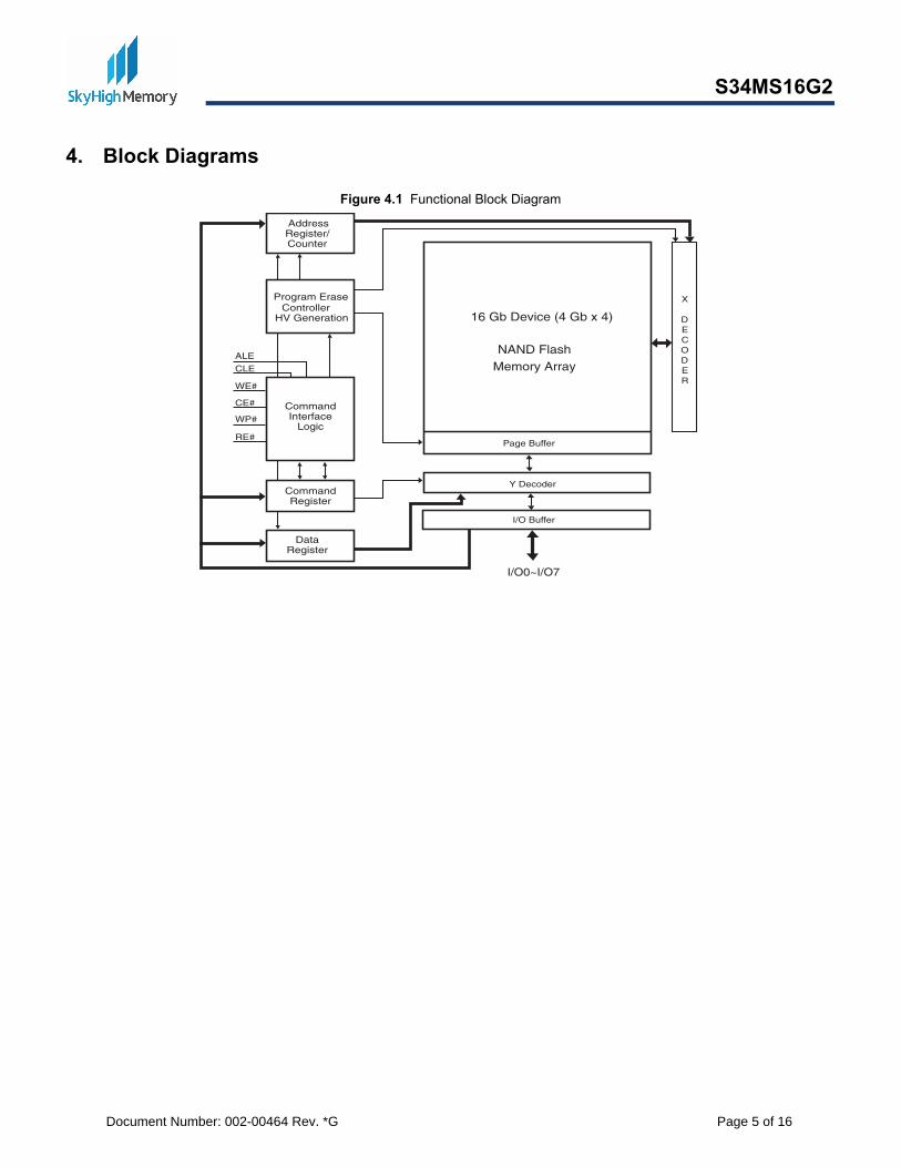
4. Block Diagrams
Figure 4.1 Functional Block Diagram
AddressRegister/Counter
Controller
CommandInterface
Logic
CommandRegister
DataRegister
RE#
I/O Buffer
Y Decoder
Page Buffer
X
DECODER
NAND FlashMemory Array
WP#
CE#
WE#
CLE
ALE
I/O0~I/O7
Program Erase
HV Generation 16 Gb Device (4 Gb x 4)
Document Number: 002-00464 Rev. *G
Page 5 of 16
S34MS16G2
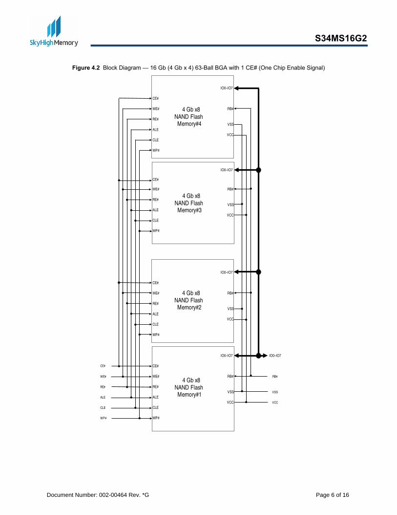
Figure 4.2 Block Diagram — 16 Gb (4 Gb x 4) 63-Ball BGA with 1 CE# (One Chip Enable Signal)
IO0~IO7
CE#
RB#WE#
RE#VSS
ALEVCC
CLE
WP#
IO0~IO7
CE#
RB#WE#
RE#VSS
ALEVCC
CLE
WP#
IO0~IO7
CE#
RB#WE#
RE#VSS
ALEVCC
CLE
WP#
IO0~IO7IO0~IO7
CE# CE#
WE# RB#WE# RB#
RE# RE#VSS VSS
ALE ALEVCC VCC
CLE CLE
WP# WP#
4 Gb x8 NAND Flash
Memory#3
4 Gb x8 NAND Flash
Memory#4
4 Gb x8 NAND Flash
Memory#1
4 Gb x8 NAND Flash
Memory#2
Document Number: 002-00464 Rev. *G
Page 6 of 16
S34MS16G2
5. Addressing
Notes:1. CAx = Column Address bit.
2. PAx = Page Address bit.
3. PLA0 = Plane Address bit zero.
4. BAx = Block Address bit.
5. Block address concatenated with page address and plane address = actual page address, also known as the row address.
6. A31 for 16 Gb (4 Gb x 4 – QDP).
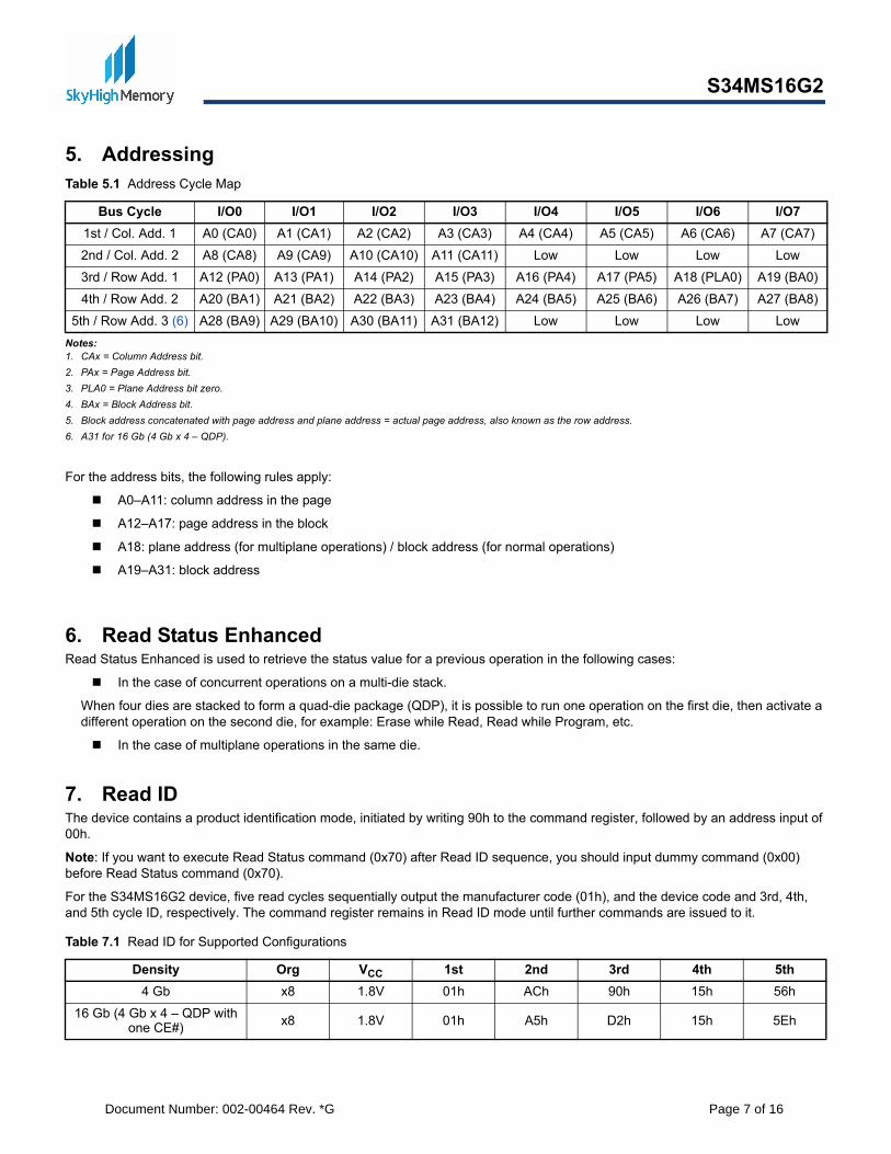
For the address bits, the following rules apply:
A0–A11: column address in the page
A12–A17: page address in the block
A18: plane address (for multiplane operations) / block address (for normal operations)
A19–A31: block address
6. Read Status EnhancedRead Status Enhanced is used to retrieve the status value for a previous operation in the following cases:
In the case of concurrent operations on a multi-die stack.
When four dies are stacked to form a quad-die package (QDP), it is possible to run one operation on the first die, then activate a different operation on the second die, for example: Erase while Read, Read while Program, etc.
In the case of multiplane operations in the same die.
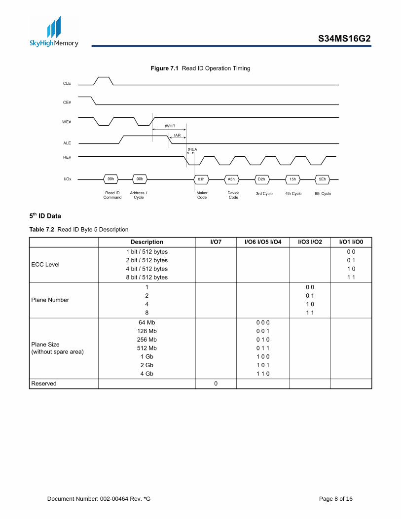
7. Read IDThe device contains a product identification mode, initiated by writing 90h to the command register, followed by an address input of 00h.
Note: If you want to execute Read Status command (0x70) after Read ID sequence, you should input dummy command (0x00) before Read Status command (0x70).
For the S34MS16G2 device, five read cycles sequentially output the manufacturer code (01h), and the device code and 3rd, 4th, and 5th cycle ID, respectively. The command register remains in Read ID mode until further commands are issued to it.
Table 5.1 Address Cycle Map
I/O7I/O6I/O5I/O4I/O3I/O2I/O1I/O0Bus Cycle
A5 (CAA4 (CA4)A3 (CA3)A2 (CA2)A1 (CA1)A0 (CA0)1st / Col. Add. 1 A7 (CA7)A6 (CA6)5)
A9 (CAA8 (CA8)2nd / Col. Add. 2 LLowLowLowA11 (CA11)A10 (CA10)9) ow
A1A16 (PA4)A15 (PA3)A14 (PA2)A13 (PA1)A12 (PA0)3rd / Row Add. 1 A19 (BA0)A18 (PLA0)7 (PA5)
A21 (A20 (BA1)4th / Row Add. 2 A2A24 (BA5)A23 (BA4)A22 (BA3)BA2) A27 (BA8)A26 (BA7)5 (BA6)
5th / Row Add. 3 (6) LowLowLowLowA31 (BA12)A30 (BA11)A29 (BA10)A28 (BA9)
Table 7.1 Read ID for Supported Configurations
VOrgDensity CC 5th4th3rd2nd1st
56h15h90hACh01h1.8Vx84 Gb
16 Gb (4 Gb x 4 – QDP with one CE#) 5Eh15hD2hA5h01h1.8Vx8
Document Number: 002-00464 Rev. *G
Page 7 of 16
S34MS16G2
Figure 7.1 Read ID Operation Timing
5th ID Data
Table 7.2 Read ID Byte 5 Description
I/O1 I/O0I/O3 I/O2I/O6 I/O5 I/O4I/O7Description
ECC Level
1 bit / 512 bytes
2 bit / 512 bytes
4 bit / 512 bytes
8 bit / 512 bytes
0 0
0 1
1 0
1 1
Plane Number
1
2
4
8
0 0
0 1
1 0
1 1
Plane Size(without spare area)
64 Mb
128 Mb
256 Mb
512 Mb
1 Gb
2 Gb
4 Gb
0 0 0
0 0 1
0 1 0
0 1 1
1 0 0
1 0 1
1 1 0
0Reserved
CE#
WE#
CLE
RE#
ALE
tWHR
tAR
tREA
Read IDCommand
Address 1Cycle
MakerCode
DeviceCode
3rd Cycle 5th Cycle4th Cycle
I/Ox 01h90h 00h 5Eh15hD2hA5h
Document Number: 002-00464 Rev. *G
Page 8 of 16

S34MS16G2
7.1 Read Parameter PageThe device supports the ONFI Read Parameter Page operation, initiated by writing ECh to the command register, followed by an address input of 00h. The command register remains in Parameter Page mode until further commands are issued to it. Table 7.3explains the parameter fields.
Note: For 32nm SkyHigh NAND, for a particular condition, the Read Parameter Page command does not give the correct values. To overcome this issue, the host must issue a Reset command before the Read Parameter Page command. Issuance of Reset before the Read Parameter Page command will provide the correct values and will not output 00h values.
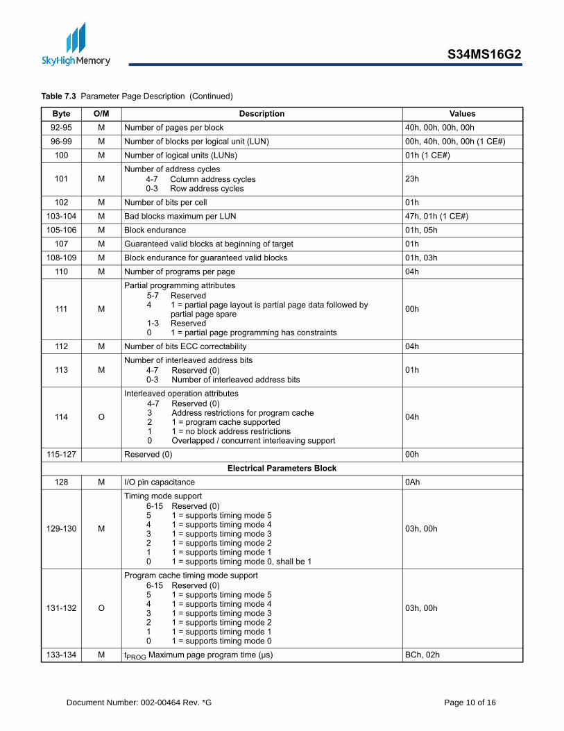
Table 7.3 Parameter Page Description
ValuesDescriptionO/MByte
Revision Information and Features Block
M0-3
Parameter page signature Byte 0: 4Fh, “O” Byte 1: 4Eh, “N” Byte 2: 46h, “F”Byte 3: 49h, “I”
4Fh, 4Eh, 46h, 49h
M4-5
Revision number 2-15 Reserved (0) 1 1 = supports ONFI version 1.0 0 Reserved (0)
02h, 00h
M6-7
Features supported 5-15 Reserved (0) 4 1 = supports odd to even page Copyback 3 1 = supports interleaved operations 2 1 = supports non-sequential page programming 1 1 = supports multiple LUN operations 0 1 = supports 16-bit data bus width
1Eh, 00h
M8-9
Optional commands supported 6-15 Reserved (0) 5 1 = supports Read Unique ID 4 1 = supports Copyback 3 1 = supports Read Status Enhanced 2 1 = supports Get Features and Set Features 1 1 = supports Read Cache commands0 1 = supports Page Cache Program command
3Bh, 00h
00hReserved (0)10-31
Manufacturer Information Block
Device manufacturer (12 ASCII characters)M32-4353h, 50h, 41h, 4Eh, 53h, 49h, 4Fh, 4Eh, 20h, 20h, 20h, 20h
Device model (20 ASCII characters)M44-63
53h, 33h, 34h, 4Dh, 53h, 31h, 36h, 47h, 32h, 20h, 20h, 20h, 20h, 20h, 20h, 20h, 20h, 20h, 20h, 20h
01hJEDEC manufacturer IDM64
00hDate codeO65-66
00hReserved (0)67-79
Memory Organization Block
Number of data bytesM80-83 00h, 08h, 00h, 00hper page
80h, 00hNumber of spare bytes per pageM84-85
Number of data bytes pM86-89 00h, 00h, 00h, 00er partial page h
00h, 00hNumber of spare bytes per partial pageM90-91
Document Number: 002-00464 Rev. *G
Page 9 of 16
S34MS16G2
Number of pagesM92-95 40h, 00h, 00h, 00hper block
Number of blocks per lM96-99 00h, 40h, 00h,ogical unit (LUN) 00h (1 CE#)
01h (1 CE#)Number of logical units (LUNs)M100
M101Number of address cycles
Column address cycles4-7Row address cycles0-3
23h
01hNumber of bits per cellM102
47h, 01h (1 CE#)Bad blocks maximum per LUNM103-104
01h, 05hBlock enduranceM105-106
Guaranteed valid blocksM107 01hat beginning of target
01h, 03hBlock endurance for guaranteed valid blocksM108-109
04hNumber of programs per pageM110
M111
Partial programming attributes Reserved5-71 = partial page la4 yout is partial page data followed by partial page spare
1-3 Reserved0 1 = partial page programming has constraints
00h
04hNumber of bits ECC correctabilityM112
M113Number of interleaved address bits
4-7 Reserved (0) 0-3 Number of interleaved address bits
01h
O114
Interleaved operation attributes 4-7 Reserved (0) 3 Address restrictions for program cache 2 1 = program cache supported 1 1 = no block address restrictions 0 Overlapped / concurrent interleaving support
04h
00hReserved (0)115-127
Electrical Parameters Block
0AhI/O pin capacitanceM128
M129-130
Timing mode support 6-15 Reserved (0) 5 1 = supports timing mode 5 4 1 = supports timing mode 4 3 1 = supports timing mode 3 2 1 = supports timing mode 2 1 1 = supports timing mode 1 0 1 = supports timing mode 0, shall be 1
03h, 00h
O131-132
Program cache timing mode support Reserved (0)6-151 = supports timing mode 55
4 1 = supports timing mode 4 3 1 = supports timing mode 3 2 1 = supports timing mode 2 1 1 = supports timing mode 1 0 1 = supports timing mode 0
03h, 00h
tM133-134 PROG BCh, 02hMaximum page program time (µs)
Table 7.3 Parameter Page Description (Continued)
ValuesDescriptionO/MByte
Document Number: 002-00464 Rev. *G
Page 10 of 16

S34MS16G2
Note: 1. “O” Stands for Optional, “M” for Mandatory.
tM135-136 BERS 10h, 27hMaximum block erase time (µs)
tM137-138 R 1Eh, 00hMaximum page read time (µs)
tM139-140 CCS Minimum Change Column s C8h, 00hetup time (ns)
00hReserved (0)141-163
Vendor Block
Vendor specifM164-165 00hic Revision number
00hVendor specific166-253
11h, F5h (1CE#)Integrity CRCM254-255
Redundant Parameter Pages
Repeat Value of bytes 0-255Value of bytes 0-255M256-511
Repeat Value of bytes 0-255Value of bytes 0-255M512-767
Additional redundanO768+ FFht parameter pages
Table 7.3 Parameter Page Description (Continued)
ValuesDescriptionO/MByte
Document Number: 002-00464 Rev. *G
Page 11 of 16
S34MS16G2
8. Electrical Characteristics
8.1 Valid Blocks
Note:1. Each 4 Gb can have a maximum 80 bad blocks.
8.2 DC Characteristics
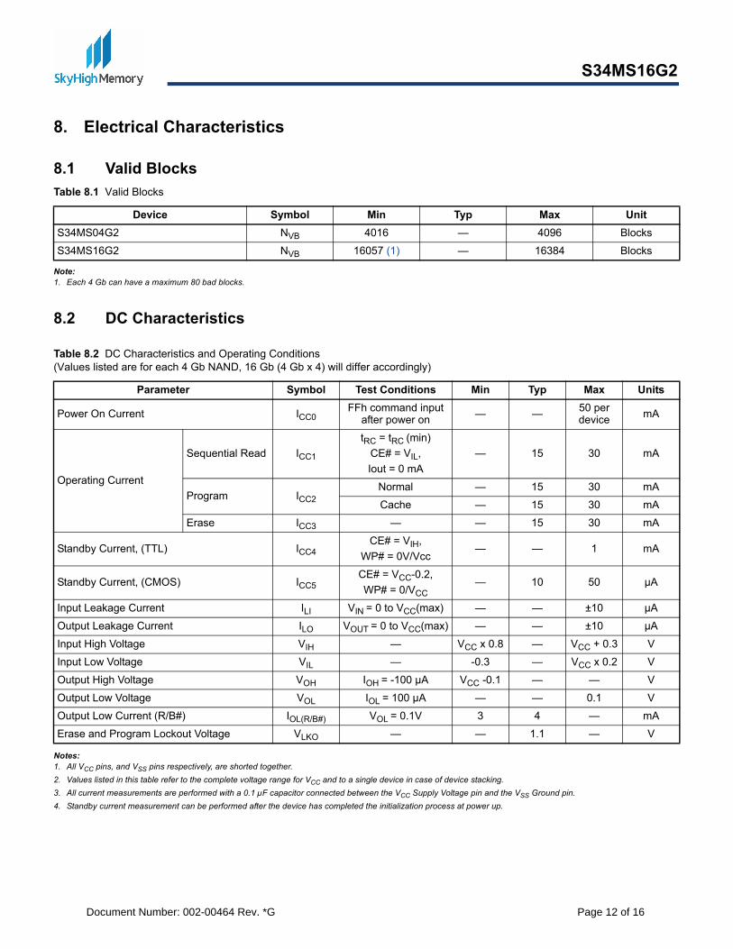
Notes:1. All VCC pins, and VSS pins respectively, are shorted together.
2. Values listed in this table refer to the complete voltage range for VCC and to a single device in case of device stacking.
3. All current measurements are performed with a 0.1 µF capacitor connected between the VCC Supply Voltage pin and the VSS Ground pin.
4. Standby current measurement can be performed after the device has completed the initialization process at power up.
Table 8.1 Valid Blocks
UnitMaxTypMinSymbolDevice
NS34MS04G2 VB — Blocks40964016
NS34MS16G2 VB 16057 (1) — Blocks16384
Table 8.2 DC Characteristics and Operating Conditions (Values listed are for each 4 Gb NAND, 16 Gb (4 Gb x 4) will differ accordingly)
UnitsMaxTypMinTest ConditionsSymbolParameter
IPower On Current CC0FFh command input
after power on ——50 per device mA
Operating Current
ISequential Read CC1
tRC = tRC (min)
CE# = VIL,
Iout = 0 mA
— mA3015
IProgram CC2— mA3015Normal
— mA3015Cache
IErase CC3 —— mA3015
IStandby Current, (TTL) CC4CE# = VIH,
WP# = 0V/Vcc—— mA1
IStandby Current, (CMOS) CC5CE# = VCC-0.2,
WP# = 0/VCC— µA5010
IInput Leakage Current LI VIN = 0 to VCC —— µA±10(max)
IOutput Leakage Current LO VOUT = 0 to VCC —— µA±10(max)
VInput High Voltage IH — VCC — Vx 0.8 CC V+ 0.3
VInput Low Voltage IL —— V-0.3 CC Vx 0.2
VOutput High Voltage OH IOH V= -100 µA CC —— V-0.1
VOutput Low Voltage OL IOL —— V0.1= 100 µA
IOutput Low Current (R/B#) OL(R/B#) VOL — mA43= 0.1V
VErase and Program Lockout Voltage LKO ——— V1.1
Document Number: 002-00464 Rev. *G
Page 12 of 16
S34MS16G2
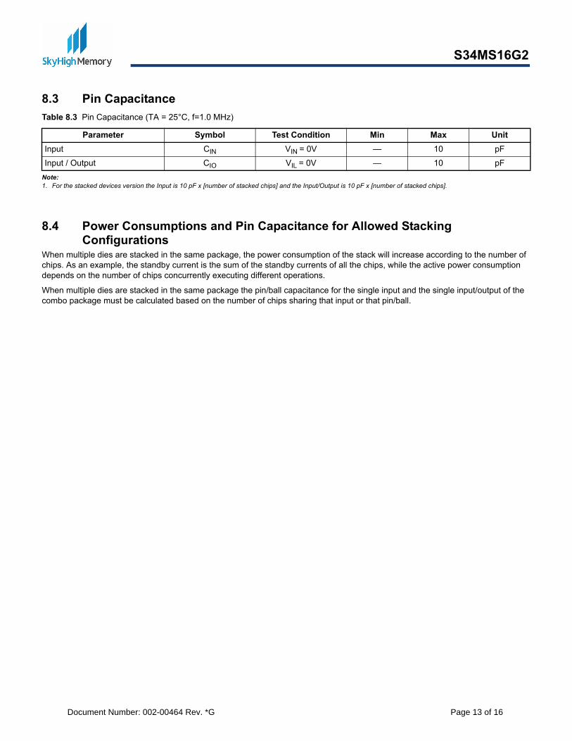
Pin Capacitance8.3
Note:1. For the stacked devices version the Input is 10 pF x [number of stacked chips] and the Input/Output is 10 pF x [number of stacked chips].
8.4 Power Consumptions and Pin Capacitance for Allowed Stacking Configurations
When multiple dies are stacked in the same package, the power consumption of the stack will increase according to the number of chips. As an example, the standby current is the sum of the standby currents of all the chips, while the active power consumption depends on the number of chips concurrently executing different operations.
When multiple dies are stacked in the same package the pin/ball capacitance for the single input and the single input/output of the combo package must be calculated based on the number of chips sharing that input or that pin/ball.
Table 8.3 Pin Capacitance (TA = 25°C, f=1.0 MHz)
UnitMaxMinTest ConditionSymbolParameter
CInput IN VIN — pF10= 0V
CInput / Output IO VIL — pF10= 0V
Document Number: 002-00464 Rev. *G
Page 13 of 16
S34MS16G2
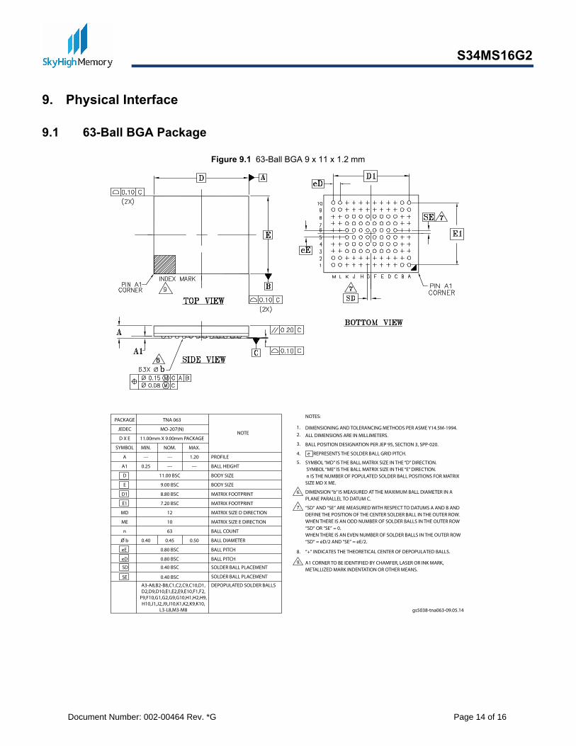
9. Physical Interface
9.1 63-Ball BGA Package
Figure 9.1 63-Ball BGA 9 x 11 x 1.2 mm
PACKAGE
JEDEC
D X E
SYMBOL
A
A1
D
E
D1
E1
MD
ME
n
O b
eE
eD
MIN.
---
0.25
0.40
A3-A8,B2-B8,C1,C2,C9,C10,D1,D2,D9,D10,E1,E2,E9,E10,F1,F2,
F9,F10,G1,G2,G9,G10,H1,H2,H9,H10,J1,J2,J9,J10,K1,K2,K9,K10,
L3-L8,M3-M8
TNA 063
MO-207(N)
11.00mm X 9.00mm PACKAGE
NOM.
---
---
11.00 BSC
9.00 BSC
8.80 BSC
7.20 BSC
12
10
63
0.45
0.80 BSC
0.80 BSC
MAX.
1.20
---
0.50
NOTE
PROFILE
BALL HEIGHT
BODY SIZE
BODY SIZE
MATRIX FOOTPRINT
MATRIX FOOTPRINT
MATRIX SIZE D DIRECTION
MATRIX SIZE E DIRECTION
BALL COUNT
BALL DIAMETER
BALL PITCH
BALL PITCH
SOLDER BALL PLACEMENT
SOLDER BALL PLACEMENT
0.40 BSCSD
gs5038-tna063-09.05.14
NOTES:
DIMENSIONING AND TOLERANCING METHODS PER ASME Y14.5M-1994.ALL DIMENSIONS ARE IN MILLIMETERS.
BALL POSITION DESIGNATION PER JEP 95, SECTION 3, SPP-020.
e REPRESENTS THE SOLDER BALL GRID PITCH.
SYMBOL “MD” IS THE BALL MATRIX SIZE IN THE “D” DIRECTION. SYMBOL “ME” IS THE BALL MATRIX SIZE IN THE “E” DIRECTION. n IS THE NUMBER OF POPULATED SOLDER BALL POSITIONS FOR MATRIXSIZE MD X ME.
DIMENSION “b” IS MEASURED AT THE MAXIMUM BALL DIAMETER IN APLANE PARALLEL TO DATUM C.
“SD” AND “SE” ARE MEASURED WITH RESPECT TO DATUMS A AND B ANDDEFINE THE POSITION OF THE CENTER SOLDER BALL IN THE OUTER ROW.WHEN THERE IS AN ODD NUMBER OF SOLDER BALLS IN THE OUTER ROW“SD” OR “SE” = 0.WHEN THERE IS AN EVEN NUMBER OF SOLDER BALLS IN THE OUTER ROW“SD” = eD/2 AND “SE” = eE/2.
A1 CORNER TO BE IDENTIFIED BY CHAMFER, LASER OR INK MARK,METALLIZED MARK INDENTATION OR OTHER MEANS.
“+” INDICATES THE THEORETICAL CENTER OF DEPOPULATED BALLS.
1.2.
3.
4.
5.
6.
7.
8.
9.
0.40 BSCSE
DEPOPULATED SOLDER BALLS
Document Number: 002-00464 Rev. *G
Page 14 of 16
S34MS16G2
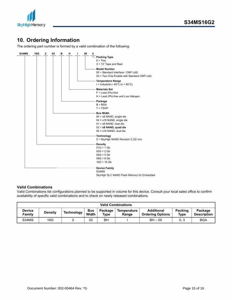
10. Ordering InformationThe ordering part number is formed by a valid combination of the following:
Valid CombinationsValid Combinations list configurations planned to be supported in volume for this device. Consult your local sales office to confirm availability of specific valid combinations and to check on newly released combinations.
000IHB02216GS34MSPacking Type0 = Tray3 = 13” Tape and Reel
Model Number00 = Standard Interface / ONFI (x8)20 = Two Chip Enable with Standard ONFI (x8)
Temperature RangeI = Industrial (–40°C to + 85°C)
Materials SetF = Lead (Pb)-freeH = Lead (Pb)-free and Low Halogen
PackageB = BGAT = TSOP
Bus Width00 = x8 NAND, single die04 = x16 NAND, single die01 = x8 NAND, dual die02 = x8 NAND, quad die05 = x16 NAND, dual die
Technology2 = SkyHigh NAND Revision 2 (32 nm)
Density01G = 1 Gb02G = 2 Gb04G = 4 Gb08G = 8 Gb16G = 16 Gb
Device FamilyS34MSSkyHigh SLC NAND Flash Memory for Embedded
Valid Combinations
Device Family
TechnologyDensity Bus Width
Package Type
Temperature Range
Additional Ordering Options
Packing Type
Package Description
BGA0, 3BH – 00IBH02216GS34MS
Document Number: 002-00464 Rev. *G
Page 15 of 16

S34MS16G2
11. Revision History
Document History Page
Document Title: S34MS16G2, 16 Gb, 4-Bit ECC, x8 I/O, and 1.8 V VCC NAND Flash for EmbeddedDocument Number: 002-00464
Rev. ECN No. Orig. of Change
Submission Date Description of Change
Initial release12/12/2014XILA–**
Performance: Corrected Package Options for 63-04/24/2015XILA–*A Ball BGA to 9 x 11 x 1.2 mmPhysical Interface: Corrected figure title to ‘63-Ball BGA 9 x 11 x 1.2 mm’Ordering Information: Ordering Information table: corrected Model Number and Materials Set
Updated to Cypress template.10/14/2015XILA4962771*B
Changed status from Advance to Final.04/28/2016XILA5244672*CUpdated Read ID:Updated Read Parameter Page:Updated description.Updated to new template.
Updated10/27/2016XILA5497766*D Electrical Characteristics:Updated DC Characteristics:Updated Table 8.2. Updated Notes 1 and 2.Updated to new template.
Updated logo and Copyright.11/09/2017AESATMP85962114*E
Updated to new template.03/16/2018MNAD6100827*FCompleting Sunset Review.
*G MNAD 05/22/2019 Updated to SkyHigh format.
Document Number: 002-00464 Rev. *G
Page 16 of 16