
pds 2u 6-1-0neo.dmcs.pl/pium/instrukcje/pds_2u_6-1-0.pdf · D is a diac, DB3, Th is a triac,...
30
Politechnika Łódzka Katedra Mikroelektroniki i Technik Informatycznych 90-924 Łódź, ul. Wólczańska 221/223, bud. B18 tel. 42 631 26 28 faks 42 636 03 27 e-mail [email protected] http://www.dmcs.p.lodz.pl POWER DEVICES AND SYSTEMS LABORATORY Exercise 2U AC voltage controller using phase control Thyristors Parameters of power electronic converters Caution! Dangerous voltages occur in the measurement set-up. Danger of shock if safety guidelines given are not followed! Exercise and manual elaborated by Łukasz Starzak Łódź 2018 ver. 6.1.0. 9/11/2018
Transcript of pds 2u 6-1-0neo.dmcs.pl/pium/instrukcje/pds_2u_6-1-0.pdf · D is a diac, DB3, Th is a triac,...

Politechnika Łódzka Katedra Mikroelektroniki i Technik Informatycznych
90-924 Łódź, ul. Wólczańska 221/223, bud. B18 tel. 42 631 26 28 faks 42 636 03 27 e-mail [email protected]
http://www.dmcs.p.lodz.pl
POWER DEVICES AND SYSTEMS LABORATORY
Exercise 2U
AC voltage controller using phase control
Thyristors Parameters of power electronic
converters
Caution! Dangerous voltages occur in the measurement set-up. Danger of shock if safety guidelines given are not followed!
Exercise and manual elaborated by Łukasz Starzak
Łódź 2018
ver. 6.1.0. 9/11/2018


© 2018 Łukasz Starzak, Katedra Mikroelektroniki i Technik Informatycznych Politechniki Łódzkiej
Contents
B Exercise Introduction ....................................................................................................................... 5
1. Exercise Aim and Plan ......................................................................................................................................... 5
2. Thyristors ............................................................................................................................................................... 7
2.1. Recommended reading ............................................................................................................................. 7
3. AC/AC Converter ................................................................................................................................................. 9
3.1. Recommended reading ............................................................................................................................. 9
3.2. Controlling the incandescent lamp using an electronic power converter ................................ 10
3.2.a. Efficiency ................................................................................................................................. 10
3.2.b. Practical concept of a complete AC voltage phase controller ................................... 11
3.2.c. The role of the RC divider................................................................................................... 12
3.2.d. The role of the diac ............................................................................................................... 14
3.2.e. Modified circuit ..................................................................................................................... 15
3.3. Controlling an incandescent lamp using electrical elements ....................................................... 17
3.3.a. Controller requirements ...................................................................................................... 17
3.3.b. Control with a variable resistor ........................................................................................ 17
3.3.c. Efficiency and power factor of the resistor-based circuit ........................................... 19
C Experiment ....................................................................................................................................... 21
4. Measurements and Simulations ...................................................................................................................... 21
4.1. Measurement set-up ............................................................................................................................... 21
Set-up description ............................................................................................................................ 21
Operation and usage of the multimeter with wattmeter function ..................................... 22
4.2. Setting up the circuit .............................................................................................................................. 23
4.3. Carrying out measurements ................................................................................................................. 24
Power conversion characteristics ................................................................................................ 24
Time-domain operation ................................................................................................................. 25
Concluding the investigation ....................................................................................................... 26
D Results .............................................................................................................................................. 27
5. Processing Results .............................................................................................................................................. 27
5.1. Electrical characteristics ........................................................................................................................ 27
Control characteristics ................................................................................................................... 27
Receiver character ........................................................................................................................... 27
Effect of receiver’s nonlinearity on converter characteristics ............................................. 28
Output power control principle ................................................................................................... 28
Power conversion quality .............................................................................................................. 28
5.2. Triac in the electronic converter ......................................................................................................... 28
E Information ...................................................................................................................................... 29
6. Required Knowledge .......................................................................................................................................... 29
6.1. Prerequisites ............................................................................................................................................. 29
6.2. Test scope .................................................................................................................................................. 29
7. References ............................................................................................................................................................ 30

© 2018 Łukasz Starzak, Katedra Mikroelektroniki i Technik Informatycznych Politechniki Łódzkiej
B
Exercise Introduction
1. Exercise Aim and Plan
The aim of this exercise is to investigate operation and characteristics of a typical AC/AC converter: an AC voltage controller using the phase angle control method. In the specific case under analysis, it will perform the task of a halogen lamp dimmer.
In this circuit, the bidirectional thyristor, or the triac, will be used as the semiconductor switch. This exercise will thus create an opportunity to get acquainted with this group of devices as well as with a related one, the diac.
References given provide an extensive description of these devices for the sake of completeness and equivalency between the English and the Polish manuals. However, this is excessive for this course as details of thyristor operation are not of high interest in this exercise.


© 2018 Łukasz Starzak, Katedra Mikroelektroniki i Technik Informatycznych Politechniki Łódzkiej
2. Thyristors
2.1. Recommended reading
Ref. Textbook Excerpt Equivalent in the
Polish Manual Complementary
Reading Complements in this Manual
A Ben 7, 7.1.1, 7.1.2, 7.1.4 2.1 [12] Thyristor and Triac
Ratings; Thyristor and Triac Characteristics
B Ben 7.2 2.2
C Ben 7.3, 7.3.1, 7.3.2, 7.3.3, 7.4.1, 7.4.2
2.3
D Ben 8.4 2.4 [11] 1.2, 1.3.1 [12] High Commutation
Triacs
E Moo 1.8.1 2.5.c


© 2018 Łukasz Starzak, Katedra Mikroelektroniki i Technik Informatycznych Politechniki Łódzkiej
3. AC/AC Converter
3.1. Recommended reading
Ref. Textbook Excerpt Equivalent in the
Polish Manual Complementary
Reading Complements in this Manual
F Moo 4.2.4 3.2.a
G Moo 4.3.1 3.2.b—c,e
3.2.d 3.2.a
3.3 3.2.b—e
3.1 3.3

10 B 3 Power Devices and Systems – Exercise 2U. AC voltage controller using phase control (6.1.0)
© 2018 Łukasz Starzak, Katedra Mikroelektroniki i Technik Informatycznych Politechniki Łódzkiej
3.2. Controlling the incandescent lamp using an electronic power converter
3.2.a. Efficiency
If we assume that the semiconductor switch (triac) is ideal, then there is no power loss in it, because when the switch is on, its current isw = 0, and when it is off, the voltage across it usw = 0, which means that at any moment
0swswsw == uip (3.1)
so by definition
0)( avswswc === pPP (3.2)
Under this assumption from (3.31) we obtain
1o
o
co
o ==+
=P
P
PP
Pη (3.3)
Real semi-conductor switches are not ideal, though. As shown in Fig. 2c—d, they have a finite resistance Roff in the off-state and a non-zero resistance Ron in the on-state. This results in energy being lost—dissipated as heat. The instantaneous power of this loss may be estimated as follows:
(1) in the off-state (1st interval)—under the assumption that Roff >> RLp (so the entire source voltage us will be present across the switch based on the voltage divider principle):
off
2s
sw(off)R
up ≈ (3.4)
(2) in the on-state (2nd interval)—under the assumption that Ron << RLp (the value of the current resulting only from the value of RLp):
on
2
Lp
son
2sw(on) R
R
uRip
≈= (3.5)
In such a case, average power loss in the converter—considering the symmetry of half-periods of the supply voltage sinusoid—equals
+=
=
+⋅⋅=
=
+++⋅=
3
1
1
0
3
1
1
0
5
4
4
3
3
1
1
0
dd11
dd2π2
1
ddddπ2
1
2s2
Lp
on2s
off
on
2
Lp
s
off
2s
sw(on)sw(off)sw(on)sw(off)c
Ω
Ω
Ω
Ω
Ω
Ω
Ω
Ω
Ω
Ω
Ω
Ω
Ω
Ω
Ω
Ω
ΩuR
RΩu
R
ΩRR
uΩ
R
u
ΩpΩpΩpΩpP
π
(3.6)
where Ω is the phase angle corresponding to time. According to (3.31), this average power results in a decrease of converter's efficiency. As can be seen from equation (3.6), power loss is greater when the off-state resistance Roff of the switch is smaller, and when the on-state resistance Ron is greater

AC/AC Converter B 3 11
© 2018 Łukasz Starzak, Katedra Mikroelektroniki i Technik Informatycznych Politechniki Łódzkiej
and this—which is important—with respect to the load resistance. The supply voltage influences both components in the same way.
ic=isw=i
Switch
ui=us
Source
RLp Lamp
Load
us Mains
io=iLp=i
uc=usw
ii=is=i
Converter
uo=uLp
Fig. 1. Light bulb dimmer circuit based on a semi-conductor switch
a) usw i=0
uLp RLpus
b) usw=0 i
us uLp RLp
c)
Roff
i
uLp
usw
us RLp
d)
i
us
usw
Ron
uLp RLp
Fig. 2. Simplified equivalent schematic of the dimmer in two intervals of its operation: a), b) under the ideal switch assumption; c), d) with static power loss taken into account
3.2.b. Practical concept of a complete AC voltage phase controller
In the textbook, only the principal (power) circuit has been considered. We did not think about how to cause the triac to turn on at a desired—and variable—moment. This function must be performed by a separate circuit—the control one. Its task will be to generate pulses of gate current IG that will trigger the triac’s gate and turn it on.
An exemplary complete (i.e. including the principal as well as the control circuit) energy conversion system that contains an AC voltage controller is presented in Fig. 3a. The principal circuit is composed of a source (the mains) us, a receiver (the light bulb) RLp and a switch (the triac) T. On the other hand, the control circuit is composed of an RC network RdCd and a diac D. As can be seen, in this case the control circuit is directly supplied from the mains, too.
The control circuit considered here, of which the diac is an important element, is one of the simplest possible. In more exigent applications it happens to be necessary to use mains zero detection circuits, generate pulse trains (instead of single pulses), protect the triac from too high a voltage or current rise rate etc. Triac control is frequently realised using digital circuits.

12 B 3 Power Devices and Systems – Exercise 2U. AC voltage controller using phase control (6.1.0)
© 2018 Łukasz Starzak, Katedra Mikroelektroniki i Technik Informatycznych Politechniki Łódzkiej
3.2.c. The role of the RC divider
Apart from the diac, the RC network also plays an important role in the dimmer. In this case it constitutes an impedance voltage divider. Fig. 4a shows the phasor diagram for this circuit where the presence of the diac has been neglected for the moment.
The RdCd circuit may be described by means of an impedance magnitude
2
d
2dd
1
−+=C
RZω
(3.7)
and a phase angle
dd
d
1arctg
CRωϕ −= (3.8)
a)
uGT1
us Rd
uD
iG
ud
io
RLp
T uT
uC
uR
uLp
Cd
id
D
b)
iT
io
T us
uLp
D
id
RLp
ud
Rd
uC
uT
Cd
Fig. 3. Complete energy conversion system with an AC voltage phase controller using a diac-based triac control circuit: a) basic circuit; b) modified circuit
When a voltage ud, equal to the mains voltage us, is applied to the RC network, a current id flows with an rms value of
d
sd
Z
UI = (3.9)

AC/AC Converter B 3 13
© 2018 Łukasz Starzak, Katedra Mikroelektroniki i Technik Informatycznych Politechniki Łódzkiej
shifted with respect to the voltage by a phase angle of −φd. As for a capacitive network φd < 0, the phase of the current is in result greater than the phase of the voltage. Thus, the current precedes the voltage.
It is obvious that
CRd uuu += (3.10)
so uR and uC phasors add up to give the ud phasor. It is also known that the voltage across Rd resistor must be in phase with id current, and the voltage across Cd capacitor must be delayed by an angle of π/2 with respect to this current. This leads to a phasor diagram shown in Fig. 4a. The system of UR, UC and Ud phasors must form a right triangle and it is follows from geometry theorems that this triangle is inscribed in a circle with a diameter of Ud.
Based on the resulting diagram we can state that the voltage across the capacitor is shifted with respect to the mains voltage by the angle of
a)
b)
c)
Fig. 4. Operation of RdCd divider without taking into account the presence of the diac: a) phasor diagram for a large resistance (Rd > 1/ωCd); b) phasor diagram for a small resistance (Rd < 1/ωCd); c) voltage waveforms (for a large resistance—solid line and for a small resistance—dashed line)

14 B 3 Power Devices and Systems – Exercise 2U. AC voltage controller using phase control (6.1.0)
© 2018 Łukasz Starzak, Katedra Mikroelektroniki i Technik Informatycznych Politechniki Łódzkiej
dCs2
π ϕϕ −−= (3.11)
Here φd < 0 and as φCs is also negative, we conclude that uC is delayed with respect to us.
Waveforms of us and uC in the considered case are presented in Fig. 4c (in the bottom plot see the solid line). Zero crossing of the voltage uC only occurs at the angle of Ω1 and maximum uC is attained at the angle of
2
π
2
π
Cs12 +=+= ϕΩΩ (3.12)
If we make Rd smaller, the φd angle (its absolute value) increases and a greater Id current flows in the circuit as a result of impedance Zd decreasing. A smaller voltage UR appears across a smaller resistance but instead, a greater current causes a greater voltage drop UC across the capacitor. When added, phasors UR and UC must still yield the invariable supply voltage Us. Also, the angles between these phasors and the phasor Id cannot change. This leads to the phasor diagram shown in Fig. 4b.
Both equation (3.11) and the phasor diagram demonstrate that the phase shift φCs (its absolute value) decreases. Waveforms of voltages us and uC in this case are shown in Fig. 4c (in the bottom plot see the dashed line).
Let us consider two extreme cases:
(1) For Rd → ∞ the network RdCd would gain a purely resistive character so phasors Id and UR would be in phase with phasor Us (triangle’s vertice moves towards the right end of phasor Us) and φCs angle would equal −π/2. The amplitude of uC would approach zero and Ω2 (the angle of maximum uC value) would approach π;
(2) For Rd → 0 the network would gain a purely capacitive character so UC = Us (triangle’s vertice moves towards the left end of phasor Us) and φCs = 0. The amplitude of uC would approach the amplitude of us and Ω2 would approach 0.
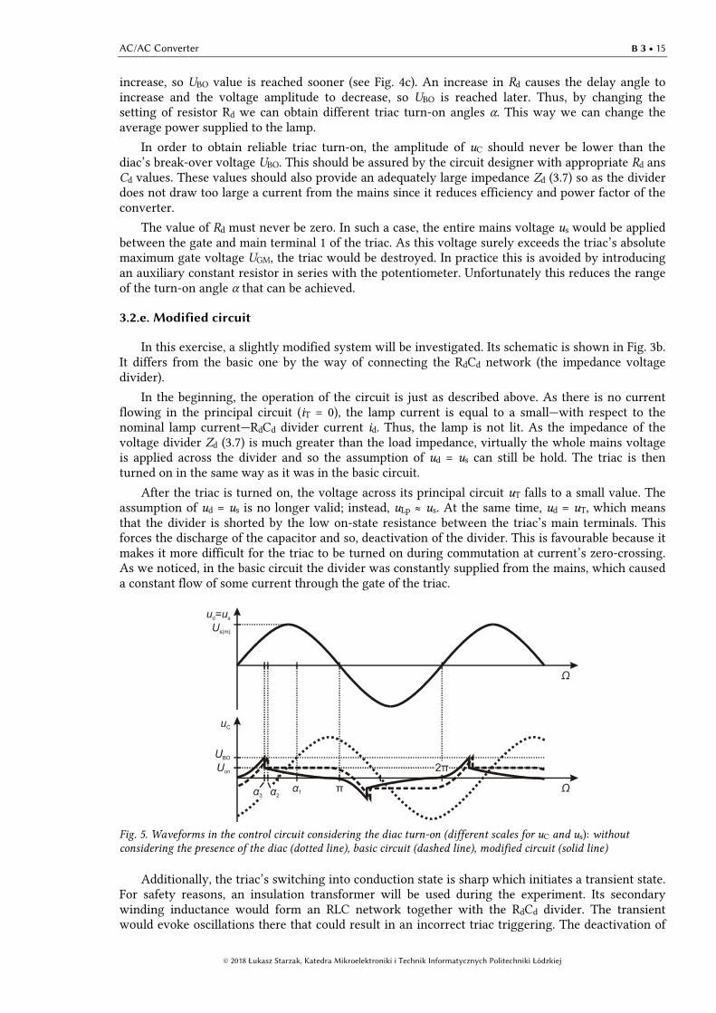
3.2.d. The role of the diac
A diac begins to conduct current after voltage across it exceeds its breakover voltage UBO which is of the order of 30 V. In the considered circuit the diac is connected between the upper terminal of the capacitor Cd and the triac’s gate. Thus, the voltage across the diac is expressed by
GT1CD uuu −= (3.13)
As no current flows in the gate circuit (excepting the neglectable diac’s leakage current), we may assume that the entire voltage uC is applied to the diac.
When the voltage uC exceeds uBO of the diac, the latter device turns on (breaks over) which means that the loop Cd–D–G–MT1 is closed. As a result, a current iG starts to flow in this loop supplied from the capacitor Cd. After some time the capacitor discharges and the current flow is stopped. If both the amplitude and the duration of current iG pulse are sufficiently large, the triac will be turned on (triggered) and a current—equal to the lamp current io—will flow between its main terminals MT2 and MT1. Thus, energy will be delivered to the lamp.
After diac turns on, the voltage across the capacitor remains constant as it equals the sum of diac’s on-state voltage Uon and triac’s gate circuit voltage uGT1.
The phase angle at which the capacitor voltage uC attains the level of diac’s break-over voltage depends on two factors:
(1) the delay angle φCs of the voltage uC with respect to the voltage us,
(2) the rise rate of the voltage uC, which results from this voltage’s amplitude.
As we concluded in our analysis of the divider RdCd, both those factors are influenced by the current value of Rd. A decrease in Rd causes the delay angle to decrease and the voltage amplitude to
AC/AC Converter B 3 15
© 2018 Łukasz Starzak, Katedra Mikroelektroniki i Technik Informatycznych Politechniki Łódzkiej
increase, so UBO value is reached sooner (see Fig. 4c). An increase in Rd causes the delay angle to increase and the voltage amplitude to decrease, so UBO is reached later. Thus, by changing the setting of resistor Rd we can obtain different triac turn-on angles α. This way we can change the average power supplied to the lamp.
In order to obtain reliable triac turn-on, the amplitude of uC should never be lower than the diac’s break-over voltage UBO. This should be assured by the circuit designer with appropriate Rd ans Cd values. These values should also provide an adequately large impedance Zd (3.7) so as the divider does not draw too large a current from the mains since it reduces efficiency and power factor of the converter.
The value of Rd must never be zero. In such a case, the entire mains voltage us would be applied between the gate and main terminal 1 of the triac. As this voltage surely exceeds the triac’s absolute maximum gate voltage UGM, the triac would be destroyed. In practice this is avoided by introducing an auxiliary constant resistor in series with the potentiometer. Unfortunately this reduces the range of the turn-on angle α that can be achieved.
3.2.e. Modified circuit
In this exercise, a slightly modified system will be investigated. Its schematic is shown in Fig. 3b. It differs from the basic one by the way of connecting the RdCd network (the impedance voltage divider).
In the beginning, the operation of the circuit is just as described above. As there is no current flowing in the principal circuit (iT = 0), the lamp current is equal to a small—with respect to the nominal lamp current—RdCd divider current id. Thus, the lamp is not lit. As the impedance of the voltage divider Zd (3.7) is much greater than the load impedance, virtually the whole mains voltage is applied across the divider and so the assumption of ud = us can still be hold. The triac is then turned on in the same way as it was in the basic circuit.
After the triac is turned on, the voltage across its principal circuit uT falls to a small value. The assumption of ud = us is no longer valid; instead, uLp ≈ us. At the same time, ud = uT, which means that the divider is shorted by the low on-state resistance between the triac’s main terminals. This forces the discharge of the capacitor and so, deactivation of the divider. This is favourable because it makes it more difficult for the triac to be turned on during commutation at current’s zero-crossing. As we noticed, in the basic circuit the divider was constantly supplied from the mains, which caused a constant flow of some current through the gate of the triac.
Fig. 5. Waveforms in the control circuit considering the diac turn-on (different scales for uC and us): without considering the presence of the diac (dotted line), basic circuit (dashed line), modified circuit (solid line)
Additionally, the triac’s switching into conduction state is sharp which initiates a transient state. For safety reasons, an insulation transformer will be used during the experiment. Its secondary winding inductance would form an RLC network together with the RdCd divider. The transient would evoke oscillations there that could result in an incorrect triac triggering. The deactivation of

16 B 3 Power Devices and Systems – Exercise 2U. AC voltage controller using phase control (6.1.0)
© 2018 Łukasz Starzak, Katedra Mikroelektroniki i Technik Informatycznych Politechniki Łódzkiej
the divider after triac turn-on prevents the oscillations from occurring and causes the voltage across the capacitor to slowly go down to zero.
It should be added that the transient state due to the diac turn-on also results in a change in the capacitor voltage waveform. After diac turn-on, the voltage uD across it is equal to some constant value, Uon. Under the assumption that uGT1 ≪ Uon, this is also equal to the voltage across the capacitor uC (Fig. 5, dashed line) unless—in the modified circuit—it has time to discharge thanks to being shorted through the triac, uC becoming equal uT ≈ 0 then (Fig. 5, solid line).
Anyway, at the beginning of a next half-period, voltage uC starts from a different level, closer to zero than what is shown in Fig. 4c and with the dotted line in Fig. 5. The diac’s break-over voltage will then be reached sooner than it has been predicted without earlier analysis. Therefore, the triac turn-on angle α will be smaller. For the basic circuit it will be α2 instead of α1 (the value for only the divider being taken into account). As in the modified circuit uC will be even closer to zero—due to the capacitor discharge—the turn-on angle α3 will be even smaller.

AC/AC Converter B 3 17
© 2018 Łukasz Starzak, Katedra Mikroelektroniki i Technik Informatycznych Politechniki Łódzkiej
3.3. Controlling an incandescent lamp using electrical elements
3.3.a. Controller requirements
In this exercise we consider the problem of controlling power of a receiver (load) supplied from the European low voltage supply network whose voltage Us is 230 V (rms value) and frequency fs is 50 Hz. The load is an incandescent lamp (a light bulb) whose nominal power PLpn is 150 W. The circuit is therefore a typical light dimmer.
When designing electronic equipment, the most important is to minimise costs and to facilitate assembly and operation. Therefore, control should be:
(1) simple (i.e. involving little elements, low cost of the elements, small dimensions and weight, low physical power), and
(2) efficient (i.e. making it possible to make maximal use of power drawn, so with high efficiency and power factor).
3.3.b. Control with a variable resistor
For the considered system, the source is the low voltage supply network which is represented with an ideal voltage source (alternating and sinusoidal) us; the load—the light bulb—is purely resistive so it may be represented with a resistor, RLp (Fig. 6). In the schematic, “i” and “o” subscripts refer to converter's input and output, “s” refers to the source (or the supply), “c” refers to the converter.
If we complement the system with a variable resistor connected in series, a voltage divider with a variable division ratio will be formed. We will describe it quantitatively now. In the circuit, a current i—as can be seen in the schematic, common to all the 3 elements—will flow. According to the Ohm's Law, its value will be
Lpp
s
RR
ui
+= (3.14)
so its rms value will be
Lpp
s
RR
UI
+= (3.15)
Also conforming to the Ohm's Law, rms value of the voltage across the lamp is expressed as
uc=up
Converter
uo=uLp
ic=ip=i
RLp Light
Bulb
us Mains
Source
ui=us
ii=is=i
Rp
Variable Resistor
io=iLp=i
Load Fig. 6. Light dimmer circuit using a variable resistor
18 B 3 Power Devices and Systems – Exercise 2U. AC voltage controller using phase control (6.1.0)
© 2018 Łukasz Starzak, Katedra Mikroelektroniki i Technik Informatycznych Politechniki Łódzkiej
Lpp
Lp
sLpLpLpLpRR
RUIRRIU
+=== (3.16)
Indeed we have obtained a resistive voltage divider, the division ratio depending on the current resistance Rp of the variable resistor.
We will now show that this way we can control the energy flow in the system. We are of course interested in the net energy flow, connected with conversion of energy into a useful form (in the considered case, light energy and—which is needless—thermal energy). This net energy flow in each period of circuit operation (in the considered case, in each mains voltage period) is characterised by the average (real) power. The light bulb being purely resistive, its average power is expressed as
2
Lpp
Lp2
sLp
2
Lpo)( RR
RURIPP
+=== (3.17)
This relationship shows that by changing the resistance Rp, we influence the power flow from source to load. Thus, the variable resistor plays the role of a converter.
A maximum lamp average power is obtained for Rp = 0 and equals
Lp
2
s
0LpLp(max)o(max)p R
UPPP
R===
= (3.18)
On the other hand, for increasing Rp we get
0pp
Lpo →=∞→∞→ RR
PP (3.19)
The relative average output power Por, defined with respect to its maximum value, is
o(max)
oΔ
orP
PP = (3.20)
which in the case under consideration yields
2
+=
+=⋅
+=
Lpp
2
Lpp
Lp
2s
Lp
2Lpp
Lp2sor
1
1
)( RRRR
R
U
R
RR
RUP (3.21)
This quantity tells what portion of the maximum possible average power will be dissipated in the light bulb for a given Rp setting. It is obviously 1 (100%) for Rp = 0 and 0 (0%) when Rp → ∞.
The results obtained point out two severe disadvantages of the considered circuit:
(1) it is not possible to get zero average output power, as in reality Rp ≠ ∞ always,
(2) the control characteristic depends on both the variable resistor and the load—which can be seen from the Por = f(Rp) relationship—so after the load is changed, this characteristic changes, too. Dimming of a 40-watt light bulb will proceed along a different curve than that for a 200-watt, i.e. for the same setting of Rp we will get a different percent of maximum average output power (as the light bulb resistance RLp will be different).
By analogy, the relative rms current value is defined as
max
Δ
rI
II = (3.22)

AC/AC Converter B 3 19
© 2018 Łukasz Starzak, Katedra Mikroelektroniki i Technik Informatycznych Politechniki Łódzkiej
which in the considered case leads to the relationship
LpPLpp
Lp
s
Lp
Lpp
s
r1
1
RRRR
R
U
R
RR
UI
+=
+=⋅
+= (3.23)
3.3.c. Efficiency and power factor of the resistor-based circuit
The quality of energy conversion is primarily described by means of efficiency
i
o
P
P=η (3.24)
It may be expected that it is not equal to 1, as the current flow through the resistor Rp produces a voltage drop across it and power dissipation in it. Thus, not all the input power gets to the load.
To calculate converter's efficiency, one must know the value of the average output power
2
Lpp
Lp
2
s
Lpo)( RR
RUPP
+== (3.25)
as well as that of the average input power which—taking into account that the load is purely resistive so there is no phase shift between current and voltage—is expressed with
Lpp
2
s
ssiRR
UIUPP
+=== (3.26)
This way we obtain the formula for the converter’s efficiency:
Lpp
Lp
2
s
Lpp
2
Lpp
Lp
2
s
i
o
)( RR
R
U
RR
RR
RU
P
P
+=
++
==η (3.27)
By analysis of (3.17) and (3.27) we can easily state that increasing the variable resistor’s resistance leads to a decrease in the average power delivered to the lamp (so enables dimming) but at the same time it decreases efficiency. For extreme settings we obtain:
for Rp = 0: the maximum lamp average power
Lp
2
s
Lp(max)LpR
UPP == (3.28)
which by definition equals the nominal power PLpn (assuming the lamp is supplied with a voltage Us equal to its nominal one), and the efficiency η = 1;
for Rp → ∞: PLp → 0 and η → 0;
and the efficiency is halved for Rp = RLp, when the output power equals 1/4 of the maximal one.
The decrease of efficiency results from an increase of power loss in the converter, i.e. increase of power dissipated in the variable resistor. This power equals
2
Lpp
p2sp
2p
)( RR
RURIP
+== (3.29)
20 B 3 Power Devices and Systems – Exercise 2U. AC voltage controller using phase control (6.1.0)
© 2018 Łukasz Starzak, Katedra Mikroelektroniki i Technik Informatycznych Politechniki Łódzkiej
so it is a decreasing function of Rp. However, it is not the absolute value which is important here, but rather the relative one, calculated with respect to the power delivered to the lamp. A comparison of (3.29) and (3.17) lets us see that in both cases the nominator increases in the same way, however the numerator stays constant for the lamp but increases for the variable resistor. Thus, in the variable resistor (the converter) more and more power is lost—with respect to the amount delivered to the lamp (the load):
ż
p
Lp2s
2Lpp
2Lpp
p2s
Lp
p
o
c)(
)( R
R
RU
RR
RR
RU
P
P
P
P=
+
+== (3.30)
This in turn results in a decrease in efficiency according to the formula
o
cco
o
1
1
P
PPP
P
+=
+=η (3.31)
which is derived from (3.24) taking into account that all the input power Pi is either delivered to the load (in a part that amounts Po) or lost in the converter (in another part, which amounts Pc):
coi PPP += (3.32)
A second parameter important for assessment of electric power conversion quality is the power factor
ii
i
IU
P=λ (3.33)
For the considered converter-receiver system this equals
1
1
Lpp
s
s
Lpp
2
s
s
s =
+⋅
+==
−
RR
UU
RR
U
IU
Pλ (3.34)
Thus, the considered system loads the supply network in an optimal way. All the electrical energy circulating in the circuit is converted to another form of energy (useful—as lamp light, or needless—as the heat dissipated both in the lamp and in the variable resistor). Putting it differently, converter’s average (real) input power and apparent input power are equal and there is no reactive power flow.

© 2018 Łukasz Starzak, Katedra Mikroelektroniki i Technik Informatycznych Politechniki Łódzkiej
C
Experiment
4. Measurements and Simulations
4.1. Measurement set-up
Set-up description
The moment when you should begin connecting the set-up is clearly marked later in this manual. Do not start before you get acquainted with all the preceding information or before completing preceding tasks.
The circuit under investigation together with necessary meters is shown in Fig. 7 where:
Lp is an incandescent lamp, Pn = 150 W, Un = 230 V,
Rp is a potentiometer, 470 kΩ, Pn = 1/4 W,
Raux is an auxiliary resistor 10 kΩ, Pn = 1/4 W,
C is a film capacitor, 100 nF, Un = 250 V (AC) or 630 V (DC),
D is a diac, DB3,
Th is a triac, BT136-600,
W1 is a digital multimeter with wattmeter function (M-3860M),
V2 is a true rms digital voltmeter (M3660D).
The circuit will be supplied with an AC voltage ui from the 230 V, 50 Hz supply network through an insulation transformer with a voltage ratio of approximately 1:1.

22 C 4 Power Devices and Systems – Exercise 2U. AC voltage controller using phase control (6.1.0)
© 2018 Łukasz Starzak, Katedra Mikroelektroniki i Technik Informatycznych Politechniki Łódzkiej
po
Lpuo
Halogen
Lamp
Double
SocketV V2
RD
RD
i
Transformer
Secondary Side
Attachment
Plug
W
W1, A1, V1
DC
Raux
Rp
piui
Th
Attachment
Socket
YE
YE
YE
RD
RD
GN GN
BU
BU
Fig. 7. Electrical schematic of the circuit under investigation
Operation and usage of the multimeter with wattmeter function
The operation of the wattmeter used is based on simultaneous recording of instantaneous current and voltage values at a given location within a circuit at consecutive moments of time. These data are processed including multiplication and averaging, resulting in the average power. The length of the averaging interval is of the order of hundreds of milliseconds, which results in an apparent delay between the measurement and the result being displayed; you should keep this in mind while setting output power.
It follows from the above that both the ammeter and the voltmeter internal circuits must be used to measure power. Their proper connection has been made easier with an attachment in the plug-and-socket form with a side connection to the multimeter. The plug of the attachment is connected to the power source whereas the further part of the circuit (i.e., the part on the receiver’s side) is plugged in its socket. The multimeter connector is a three-terminal plug which should be inserted into the meter’s sockets so that labels on the connector and on the meter’s casing are consistent with each other.
As recording of both voltage and current samples is necessary for power measurement, the multimeter can additionally calculate the rms value of the input current (which is symbolised by A1 in Fig. 7) and the rms value of the input voltage (V1). When the multimeter used operates in wattmeter mode, it displays all the three values (average power, rms current and rms voltage) simultaneously on its screen.

Measurements and Simulations C 4 23
© 2018 Łukasz Starzak, Katedra Mikroelektroniki i Technik Informatycznych Politechniki Łódzkiej
4.2. Setting up the circuit
1. Plug off the white extension cord from the mains and free all its sockets. Plug the transformer’s primary side plug through a soft start device into one of the extension cord’s sockets. Leave the transformer’s secondary side socket unoccupied.
2. Assuming the light bulb is a purely resistive receiver, based on the formula for average power of a resistive two-terminal device, calculate the rms value of the current that will flow in the circuit after supplying it from the 230 V mains when the triac is turned on, supposing it is an ideal switch (zero voltage between its main terminals).
3. Leave the meters switched off for the moment.
4. Make connections in the circuit according to the figure and the following guidelines (still without plugging the extension cord to the mains or the wattmeter’s attachment to the transformer’s secondary side socket):
If a plug jams in a socket, don’t draw it by force but rather spin around and gently pull up at the same time. Otherwise the plug will be damaged.
(a) Use wires with insulated (with the exception of wires connecting to standard grid sockets) plugs that contain an extra vertical socket enabling to make multiple connections at one point.
(b) Apply colours as shown in Fig. 7:
yellow (YE) and red (RD) for the high-voltage part,
green (GN) for the triac gate circuit,
blue (BU) for the rest of the control circuit.
(c) First connect the current circuit—along the path of the principal current i (marked in bold in Fig. 7). Only afterwards wire the control sub-circuit and connect the voltmeter.
(d) Use meter sockets appropriate for functions used and for circuit data given above and determined in step 2.
5. Set the wiper of the variable resistor approximately in the middle of its range.
6. Ask the instructor to check your connections. In the meantime, continue with steps 7 to 9;
7. Turn on the computer. After logon completes, turn on the oscilloscope and, if necessary, configure its connection to the computer following the manual available at the laboratory stand.
8. Using the oscilloscope communication application, upload initial settings to the oscilloscope:
go to the Get & Send Settings tab;
click Open and read the file ustawienia_2u_tbs1052.set;
click Send Settings (not Send to multiple);
return to the Screen Capture tab.
9. Prepare the current probe for use:
(a) detach any voltage probes from the oscilloscope;
(b) attach the current probe to the oscilloscope’s channel 1 following the procedure described in a manual available at the laboratory stand;
(c) set up the current probe following the procedure described in the manual;
(d) clamp the probe around any wire leading the principal (lamp) current i (direction is unimportant in this case as the measured current is an alternating one).

24 C 4 Power Devices and Systems – Exercise 2U. AC voltage controller using phase control (6.1.0)
© 2018 Łukasz Starzak, Katedra Mikroelektroniki i Technik Informatycznych Politechniki Łódzkiej
4.3. Carrying out measurements
Power conversion characteristics
1. Turn on the meters and configure them:
(a) using the knob, select an appropriate function for the multimeter W1;
(b) using the knob, select appropriate (according to the circuit data given above) function and range for the multimeter V2;
(c) using the AC/DC button, activate the AC measurement function on the multimeter V2 (activation is indicated as “AC” in the display).
If the abovementioned meter turns off during measurements, the abovementioned function must be re-activated after the meter is turned back on. Otherwise results obtained will be useless.
If the battery discharge indicator (a battery symbol) shows up on any meter’s display, do not continue measurements, but ask the teacher to replace the battery. Otherwise meter indications may become erroneous.
While performing measurements:
Do not touch any parts of the measurement set-up when it is energised. Particularly do not touch elements placed between the top and bottom plates of component blocks nor the metal casing of the halogen lamp. Risk of shock!
Don’t make any switch-overs in the circuit when it is energised!
Always disconnect the circuit from the mains by plugging the wattmeter’s attachment off the transformer’s secondary side socket. The transformer may stay connected to the mains provided safety measures are applied, including not touching it.
Warning!
Before proceeding any further, it is obligatory to obtain an explicit acceptance of your wiring from the instructor.
2. Plug the white extension cord into the main power strip at the laboratory stand. Plug the wattmeter’s attachment into the transformer’s secondary side socket.
3. Ensure that one period of a current waveform conforming to the operating principle of the circuit under investigation has appeared on the oscilloscope’s screen. It may be necessary to check a different dimmer potentiometer setting as well as to adjust oscilloscope settings:
(a) set the time base, i.e. the horizontal scale (Horizontal Scale knob), so that one waveform period can be observed on the screen;
(b) set channel 1 gain, i.e. its vertical scale (Vertical Scale knob), so that the waveform fills the screen vertically to the maximum extent but without extending beyond it.
4. Set the potentiometer in the position resulting in the maximum output power (and thus, to the maximum illuminance).
5. For 10 to 15 points roughly evenly distributed between the extreme settings of the potentiometer’s wiper (these extreme positions included), measure and write down:
For each measurement point, all the sub-steps below must be executed before proceeding to a following measurement point!
(a) average input power Pi, which is the indication of the meter W1;
As mentioned in Sub-chapter 4.1, while the multimeter W1 operates in its wattmeter mode, it simultaneously displays average power, rms current and rms voltage on its screen. Thus, in order

Measurements and Simulations C 4 25
© 2018 Łukasz Starzak, Katedra Mikroelektroniki i Technik Informatycznych Politechniki Łódzkiej
to read out rms current or voltage, the multimeter’s operating mode should not be changed with the knob to ammeter or voltmeter.
According to the operating principle of the digital wattmeter described in Sub-chapter 4.1, its indication is refreshed in relatively long time steps. After power in the circuit changes, the appropriate new indication is only obtained after it stabilises, which may take up to a few seconds.
(b) rms current I, which is the indication of the meter A1;
(c) rms input voltage Ui, which is the indication of the meter V1;
(d) rms output (lamp) voltage Uo, which is the indication of the meter V2;
(e) the time interval ∆tα corresponding to the triac turn-on delay phase angle α, using the oscilloscope as described below:
push the Cursor button;
if needed, use the first top button next to the screen and the Multipurpose knob to select Type: Time;
if needed, use the second button next to the screen and the Multipurpose knob to select Source: Ch1;
with an appropriate button next to the screen choose Cursor1 and move cursor 1 with the Multipurpose knob, then acting by analogy with cursor 2, so as the cursors enclose the interval where current does not flow;
the ∆ … s indication on the right-hand side of the screen is the ∆tα interval length requested.
Upon completion of the above step, ensure that data for a measurement point corresponding to the maximum output power have been recorded.
Time-domain operation
6. Set the potentiometer Rp in a position resulting in the maximum output power. Write down the indications of A1 (rms current I) and V2. Using these values, calculate the present (thus, the maximum) average output power Po(max).
7. Adjust the time base of the oscilloscope (Horizontal Scale) so as 2 to 4 waveform periods can be observed on the screen.
8. Download the waveform image to the computer and save it to a file:
in the OpenChoice Desktop application, go to the Screen Capture tab,
click Get Screen;
click Save As,
in the Save as format field, select PNG,
choose a location for the file and give it a name,
accept with the mouse (not with the Enter key, as this would cause another activation of the Save As button).
9. Without making any changes in the circuit, on the current probe or on the oscilloscope, set the potentiometer Rp so that the average output power equals about 50% of its maximum value calculated in step 6. A present average output power should be calculated as before, based on indications of A1 and V2. As an estimate, you may initially use the value of Pi indicated by the wattmeter W1.
10. Repeat step 8.
11. Write down present rms current I and average output power Po.
12. Unclamp the current probe from the conductor. If the probe is battery-powered, turn it off with the ON/OFF switch.

26 C 4 Power Devices and Systems – Exercise 2U. AC voltage controller using phase control (6.1.0)
© 2018 Łukasz Starzak, Katedra Mikroelektroniki i Technik Informatycznych Politechniki Łódzkiej
Concluding the investigation
13. Disconnect the circuit from the mains in the following order:
(a) plug the wattmeter’s attachment off the transformer’s secondary side socket;
(b) plug the extension cord off the main power strip;
(c) plug the transformer’s plug, together with the soft start device, off the extension cord.
14. Remove remaining connections.

© 2018 Łukasz Starzak, Katedra Mikroelektroniki i Technik Informatycznych Politechniki Łódzkiej
D
Results
5. Processing Results
5.1. Electrical characteristics
Control characteristics
1. For each measurement point, calculate:
(a) triac turn-on delay phase angle α, using the ∆tα interval length measured and the known mains frequency, based on the proportion
s
π2
Δ Tt=
α
α (5.1)
where Ts is the mains period; after obtaining the result in radians, convert it to degrees and use the latter unit later on;
(b) apparent input power Si, from its definition (see Manual 0, Ref. D), using the measured values of current I and voltage Ui;
(c) average output power Po, using Uo and I values measured and considering that an incandescent lamp is a purely resistive receiver (φ = 0; see Manual 0, Ref. D);
(d) relative rms current Ir, from its definition (3.22), assuming that the maximum value is identical with the maximum measured one;
(e) relative average output power Por, from its definition (3.20), assuming that the maximum value is identical with the maximum measured one;
(f) lamp resistance Rlp, using Uo and I values measured.
2. Fill in Part 1 of the report (leave η and λ columns in the result table unfilled for now).
Receiver character
3. Fill in Part 2 of the report.

28 D 5 Power Devices and Systems – Exercise 2U. AC voltage controller using phase control (6.1.0)
© 2018 Łukasz Starzak, Katedra Mikroelektroniki i Technik Informatycznych Politechniki Łódzkiej
Effect of receiver’s nonlinearity on converter characteristics
4. * Fill in Part 3 of the report.
Output power control principle
5. Fill in Part 4 of the report.
Power conversion quality
6. For each measurement point, calculate:
(a) converter efficiency η, from its definition (see Manual 0, Ref. B);
(b) converter-load system power factor λ, from its definition (see Manual 0, Ref. D).
7. Add results obtained to the table in Part 1 of the report. Add formulae used in the space provided for this purpose.
8. Fill in Part 5 of the report.
5.2. Triac in the electronic converter
1. Fill in Part 6 of the report.

© 2018 Łukasz Starzak, Katedra Mikroelektroniki i Technik Informatycznych Politechniki Łódzkiej
E
Information
6. Required Knowledge
6.1. Prerequisites
Schematic and general principle of operation of the AC voltage controller using phase control (from the principal circuit point of view only, disregarding the control circuit). (Ref. F and Section 3.2.b)
6.2. Test scope
1. Instantaneous electrical power. Average power definition and its relationship to instantaneous power. Root-mean-square value definition. Average power of a resistive receiver. (Manual 0, Ref. C)
2. Apparent power, reactive power and power factor. Interpretation and importance of the different power quantities. Generic formulae and values for a linear inductive load (phase angle-based formulae). Efficiency and motivations for increasing it. (Manual 0, Refs. B and D)
3. Schematic and general principle of operation of AC voltage controller using phase control (from the principal circuit point of view only, disregarding the control circuit). Characteristics of: average output power, power factor and efficiency (graphical form, without formulae). Advantages and drawbacks for the final consumer and for the owner of the power distribution network. (Refs. F and G, Sections 3.2 and 3.3.a; report)
4. Thyristors. Symbol, main terminals, control (drive) terminal. Static characteristics of the principal circuit including operating states for an SCR and for a triac. Characteristics of the particular states (how they manifest externally, without considering physical phenomena inside a structure). (Ref. A and Manual 0, Ref. H)
5. Thyristor turn-on and turn-off mechanisms (from the point of view of voltages and currents observed at device terminals, without describing physical phenomena inside a structure). Mechanisms observed in the converter investigated. (Refs. B, C and D; report)

30 E 7 Power Devices and Systems – Exercise 2U. AC voltage controller using phase control (6.1.0)
© 2018 Łukasz Starzak, Katedra Mikroelektroniki i Technik Informatycznych Politechniki Łódzkiej
7. References
[1] Benda V., Gowar J., Grant D. A.: Power Semiconductor Devices: Theory and Applications. Wiley, 1999. ISBN 0-471-97644-X.
[2] Moorthi V. R.: Power Electronics: Devices, Circuits, and Industrial Applications. Oxford, 2005. ISBN 0-19-567092-2.
[11] Snubberless™ and logic level TRIAC behavior at turn-off. Rev. 3. STMicroelectronics, March 2008. Application Note AN439.
[12] Thyristors and triacs: Introduction. Philips Semiconductors, February 1996.


![The Microwave Sources for EPR Spectroscopy · and c is the speed of light. The magnetron is characterized by a high instability of both a generated frequency and its phase [4]. Due](https://static.fdocuments.pl/doc/165x107/5e6876dca613c33c6b07654d/the-microwave-sources-for-epr-spectroscopy-and-c-is-the-speed-of-light-the-magnetron.jpg)