Design and computer simulations of nanodevices with ... · kowe, poniewaz_ qubit spinowy jest...
73
AKADEMIA G ´ ORNICZO - HUTNICZA im. Stanislawa Staszica w Krakowie Wydzial Fizyki i Informatyki Stosowanej UNIVERSITEIT ANTWERPEN Faculteit Wetenschappen Departement Fysica Ph.D Thesis Design and computer simulations of nanodevices with applications to quantum computing Author: mgr in˙ z. Pawel Szumniak Promotor: Prof. dr hab. Stanislaw Bednarek Co-promotor: Prof. dr. Bart Partoens June 2013
Transcript of Design and computer simulations of nanodevices with ... · kowe, poniewaz_ qubit spinowy jest...
AKADEMIA GORNICZO - HUTNICZAim. Stanis lawa Staszica w Krakowie
Wydzia l Fizyki i Informatyki Stosowanej
UNIVERSITEIT ANTWERPEN
Faculteit Wetenschappen Departement Fysica
Ph.D Thesis
Design and computer simulations ofnanodevices with applications to
quantum computing
Author:
mgr inz. Pawe l Szumniak
Promotor:
Prof. dr hab. Stanis law Bednarek
Co-promotor:
Prof. dr. Bart Partoens
June 2013
.
This dissertation is dedicated to my wonderful wife Sylwia
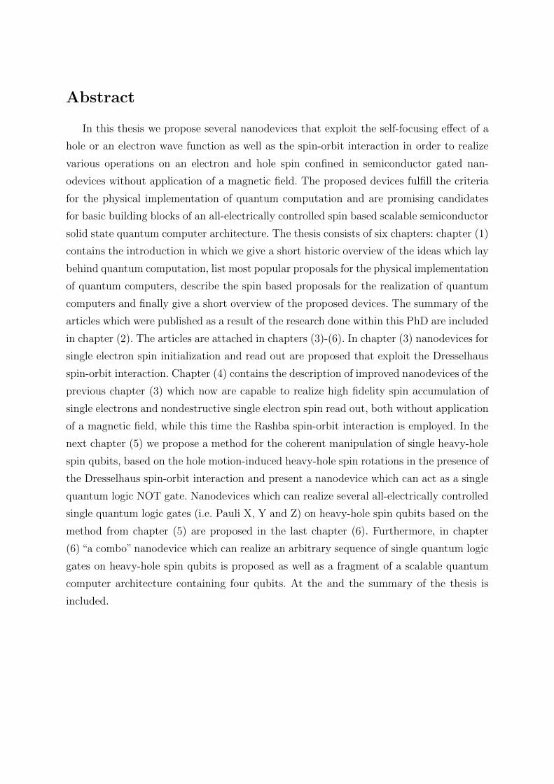
Abstract
In this thesis we propose several nanodevices that exploit the self-focusing effect of a
hole or an electron wave function as well as the spin-orbit interaction in order to realize
various operations on an electron and hole spin confined in semiconductor gated nan-
odevices without application of a magnetic field. The proposed devices fulfill the criteria
for the physical implementation of quantum computation and are promising candidates
for basic building blocks of an all-electrically controlled spin based scalable semiconductor
solid state quantum computer architecture. The thesis consists of six chapters: chapter (1)
contains the introduction in which we give a short historic overview of the ideas which lay
behind quantum computation, list most popular proposals for the physical implementation
of quantum computers, describe the spin based proposals for the realization of quantum
computers and finally give a short overview of the proposed devices. The summary of the
articles which were published as a result of the research done within this PhD are included
in chapter (2). The articles are attached in chapters (3)-(6). In chapter (3) nanodevices for
single electron spin initialization and read out are proposed that exploit the Dresselhaus
spin-orbit interaction. Chapter (4) contains the description of improved nanodevices of the
previous chapter (3) which now are capable to realize high fidelity spin accumulation of
single electrons and nondestructive single electron spin read out, both without application
of a magnetic field, while this time the Rashba spin-orbit interaction is employed. In the
next chapter (5) we propose a method for the coherent manipulation of single heavy-hole
spin qubits, based on the hole motion-induced heavy-hole spin rotations in the presence of
the Dresselhaus spin-orbit interaction and present a nanodevice which can act as a single
quantum logic NOT gate. Nanodevices which can realize several all-electrically controlled
single quantum logic gates (i.e. Pauli X, Y and Z) on heavy-hole spin qubits based on the
method from chapter (5) are proposed in the last chapter (6). Furthermore, in chapter
(6) “a combo” nanodevice which can realize an arbitrary sequence of single quantum logic
gates on heavy-hole spin qubits is proposed as well as a fragment of a scalable quantum
computer architecture containing four qubits. At the and the summary of the thesis is
included.
Streszczenie
Niniejsza praca dotyczy projektowania i symuluacji dzia lania nanourz ↪adzen wykonuj ↪a-
cych kwantowe operacje logiczne na spinie elektronu (dziury) uwi ↪ezionego w po lprzewod-
nikowej nanostrukturze bez koniecznosci stosowania pola magnetycznego. Wykorzystany
jest w nich efekt samoogniskowania funkcji falowej elektronu lub dziury oraz oddzia lywa-
nie spin-orbita. Zaproponowane nanourz ↪adzenia spe lniaj ↪a kryteria fizycznej implementacji
komputerow kwantowych i s ↪a bardzo obiecuj ↪acymi kandydatami na podstawowe elementy
skalowalnej architektury komputera kwantowego opartej o nanostruktury po lprzewodni-
kowe, poniewaz qubit spinowy jest kontrolowany wy l ↪acznie za pomoc ↪a niewielkich napi ↪ec
przyk ladanych do elektrod. Praca sk lada si ↪e z szesciu rozdzia low: w rozdziale (1) zawarty
jest wst ↪ep obejmuj ↪acy krotki rys historyczny dotycz ↪acy idei obliczen kwantowych, lista
najpopularniejszych propozycji fizycznej realizacji komputerow kwantowych ze szczegol-
nym uwzgl ↪ednieniem rozwi ↪azan wykorzystuj ↪acych jako kubit spin elektronu uwi ↪ezionego
w po lprzewodnikowych nanostrukturach. Rozdzia l konczy si ↪e krotkim opisem zapropono-
wanych w pracy nowych nanourz ↪adzen. Podsumowanie artyku low zawieraj ↪acych wyniki
uzyskane podczas realizacji doktoratu zawarte s ↪a w rozdziale (2). Publikacje tworz ↪ace dy-
sertacj ↪e zamieszczone s ↪a w rozdzia lach kolejno od (3) do (6). W rozdziale (3) dyskutowane
s ↪a nanourz ↪adzenia s luz ↪ace do ustawiania oraz do odczytu spinu pojedynczego elektronu.
Rozdzia l (4) zawiera propozycj ↪e i opis nanourzadzen zdolnych do ustawiania i nieniszcz ↪a-
cego odczytu stanu spinowego elektronu bez koniecznosci stosowania pola magnetycznego.
S ↪a one w duzym stopniu ulepszone w stosunku do nanourzadzen zaproponowanych w roz-
dziale (3). W kolejnym rozdziale (5) przedstawiamy metod ↪e wykonywania koherentnych
operacji na kubicie realizowanym przez stan spinowy dziury ci ↪ezkiej. Tego typu rozwi ↪aza-
nie jest korzystne poniewaz spin dziury ci ↪ezkiej w porownaniu do spinu elektronu cechuje
si ↪e znacznie d luzszym czasem koherencji. Proponujemy nanourz ↪adzenie wykonuj ↪ace na
spinie dziury kwantow ↪a operacj ↪e logiczn ↪a NOT. W ostatnim rozdziale (6) przedstawiona
jest propozycja nanourzadzen, ktore s ↪a w stanie wykonywac, rozne kwantowe operacje
logiczne (np. bramki Pauligo X, Y i Z) na pojedynczym dziurowym kubicie spinowym.
W rozdziale (6) zaproponowane jest ponadto nanourz ↪adzenie “combo” zdolne do wykony-
wania dowolnej sekwencji jednokubitowych operacji logicznych oraz fragment skalowalnej
architektury (zawieraj ↪acej cztery kubity) sk ladaj ↪acej si ↪e z takich nanourz ↪adzen. Na koncu
pracy znajduje si ↪e podsumowanie.
Abstract
In deze thesis stellen we een aantal nanodevices voor die gebruik maken van het zelf-
focusing effect van een holte of elektron en van de spin-baan interactive om verschillende
logische operaties te implementeren op de spin van een elektron en holte in halfgeleider
nanodevices met gates en zonder een uitwendig aangelegd magneetveld. De voorgestelde
devices voldoen aan de criteria voor de fysische implementatie van kwantumcomputatie
en zijn veelbelovende bouwstenen voor een volledig elektrostatisch gecontroleerde spin
gebaseerde schaalbare halfgeleider kwantumarchitectuur. De thesis omvat 6 hoofdstukken.
Hoofdstuk (1) geeft een inleiding met een kort historisch overzicht met de ideeen achter
kwantumcomputatie. Daarnaast bespreekt het de meest populaire voorstellen voor de
fysische implementatie van een kwantumcomputer, de spin gebaseerde voorstellen in het
bijzonder. Tot slot wordt een kort overzicht gegeven van de devices die voorgesteld worden
in deze thesis. Een samenvatting van de artikels die gepubliceerd werden voortvloeiende
uit het onderzoek dat verricht werd in dit doctoraat wordt gegeven in hoofdstuk 2. De
artikels zijn toegevoegd als hoofdstukken (3) tot (6). In hoofdstuk (3) worden de nan-
odevices voor de initialisatie en uitlezing van een enkele elektron spin voorgesteld. Deze
devices maken gebruik van de Dresselhaus spin-baan interactie.In hoofdstuk (4) komen
verbeterde versies van deze nanodevices aan bod komen die het mogelijk maken om de
spin van een elektron niet-destructief uit te lezen, en dit zonder gebruik te maken van
een uitwendig aangelegd magneetveld. Hierbij wordt gebruik gemaakt van de Rashba
spin-baan koppeling. In het volgende hoofdstuk (5) stellen we een methode voor voor de
coherente manipulatie van een enkele heavy-hole qubit, gebaseerd op de beweging van de
holte door geınduceerde holte spin rotaties door de aanwezigheid van de Dresselhaus spin-
baan interactie. Hier beschrijven we een nanodevice dat een kwantum logische NOT gate
realiseert. Nanodevices voor verschillende volledig elektrostatisch gecontroleerde kwantum
logische operaties(i.e. Pauli X,Y en Z) op heavy-hole spin qubits, gebruik makende van
de methode van hoofdstuk (5), worden voorgesteld in hoofdstuk (6). Bovendien wordt
in hoofdstuk (6) ook een ”combo” device voorgesteld dat in staat is om een willekeurige
sequentie van kwantum logische operaties uit te voeren op een heavy-hole qubit, en een
fragment van een schaalbare kwantumcomputerarchitectuur met vier qubits. Tot slot volgt
een samenvatting.
Acknowledgement
This thesis would not have been possible without the involvement of my promoters
prof. Stanis law Bednarek and prof. Bart Partoens to whom I wish to express my sincere
gratitude. On this page I would like to thank them for giving me an unique opportunity to
work on interesting research topics, for their motivation, invaluable support and guidance
during my PhD studies. This thesis is a result of their consistent encouragement and the
fruitful discussions I had with them. It was a great privilege for me to work with them.
I would like to thank all my colleagues from the Theory of Nanostructures and Nanode-
vices Group for fruitful and interesting and very often entertaining conversations. Espe-
cially, I thank my office roommates: Micha l Nowak (actual) and Przemys law Grynkiewicz
(former), conference and lunch companions: Micha l Zegrodnik, Pawe l Wojcik, Jaros law
Paw lowski and W. Pasek who have provided a cheerful atmosphere during the realization
of my thesis. I have spent great time with you guys. I also thank all the professors and
doctors from the NN group: prof. B. Szafran, prof. J. Adamowski, dr. T. Chwiej, and dr.
B. Spisak who were always ready to help.
Also I would like to thank prof. F. Peeters for his hospitality during my one year stay
at Antwerp University and all my colleagues from the Condensed Matter Theory group in
Antwerp with whom I have the privilege to make interesting and inspiring conversations.
The possibility to do research in your group was an unique, valuable and unforgettable
experience.
I would also like to thank Foundation for Polish Science for financial within the
“Krakow Interdisciplinary PhD Project in Nanoscience and Advanced Nanostructures”
programmes co-financed by the EU European Regional Development Fund. and the coor-
dinator prof. Bart lomiej Szafran for his exceptionally good management of the project. I
thank the NCN Polish National Science Center who also supported some part of research
done within the thesis with the Grant no. DEC-2011/03/N/ST3/02963 and PL-Grid In-
frastructure.
Finally, special thanks to my wonderful wife Sylwia for her love, encouragement and
patience, my parents Zbigniew and Barbara, for their support throughout my life and
my newborn son Jan whose smile has motivated me to work during the very end of the
preparation of this thesis.
There is one more person I would like to thank, ks. prof. Jan Zelazny, thank you for
the many inspiring discussions we had.
CONTENTS
Contents
About the thesis . . . . . . . . . . . . . . . . . . . . . . . . . . . . . . . . . . . 2
1 Introduction, motivation and context of the
thesis 3
2 Summary of the articles which forms this thesis
and conclusions 10
2.1 Article A1, Nanodevice for High Precision Readout of Electron Spin . . . . 10
2.2 Article A2, Spin accumulation and spin read out without magnetic field . . 12
2.3 Article A3, Spin-Orbit-Mediated Manipulation of Heavy-Hole Spin Qubits
in Gated Semiconductor Nanodevices . . . . . . . . . . . . . . . . . . . . . 15
2.4 Article A4, All-electrical control of quantum gates for single heavy-hole spin
qubits . . . . . . . . . . . . . . . . . . . . . . . . . . . . . . . . . . . . . . 16
3 Nanodevice for High Precision Readout of Electron Spin 18
4 Spin accumulation and spin read out without magnetic field 22
5 Spin-Orbit-Mediated Manipulation of Heavy-Hole Spin Qubits in Gated
Semiconductor Nanodevices 28
6 All-electrical control of quantum gates for single heavy-hole spin qubits 34
Summary 47
Podsumowanie 49
Samenvatting 51
Bibliography 53
1
ABOUT THE THESIS
About the thesis
The present dissertation consists of monothematic articles in which we propose several
nanodevices that exploit the soliton effect of a hole or an electron wave function as well as
the spin-orbit interaction in order to realize all-electrically controlled operations on elec-
tron and a hole spin qubits confined in gated semiconductor nanostructures for quantum
computing applications. The dissertation is composed of the following articles:
A1 P. Szumniak, S. Bednarek, P. Grynkiewicz, B. Szafran Nanodevice for High Preci-
sion Readout of Electron Spin,
Acta Physica Polonica A 119, 651 (2011).
A2 S. Bednarek, P.Szumniak, and B. Szafran Spin accumulation and spin read out
without magnetic field,
Phys. Rev. B 82, 235319 (2010).
A3 P. Szumniak, S. Bednarek, B. Partoens, and F. M. Peeters, Spin-Orbit-Mediated
Manipulation of Heavy-Hole Spin Qubits in Gated Semiconductor Nanodevices,
Phys. Rev. Lett. 109, 107201 (2012).
A4 P. Szumniak, S. Bednarek, J. Paw lowski, and B. Partoens, All-electrical control of
quantum gates for single heavy-hole spin qubits,
Phys. Rev. B 87, 195307 (2013).
The series of papers which constitute the dissertation are preceded by an introduc-
tion and a summary of the articles (which can be treated as a guide to the articles)
with a description of the novel contribution to the existing field of solid state spin based
implementation of quantum computation. At the end of the thesis a summary is included.
2
1 INTRODUCTION, MOTIVATION AND CONTEXT OF THETHESIS
1 Introduction, motivation and context of the
thesis
In 1982, preceded by some ideas related to quantum information theory [1, 2], Richard
Feynman published an original article [3] in which he suggested that the time dependent
numerical simulation of a many body quantum system will be an extremely challeng-
ing task to realize using standard computers. Together with David Deutch and other
researchers [3, 4, 5, 6] they proposed an alternative computer architecture - a quantum
computer - which exploits the basic and counterintuitive laws of quantum mechanics (such
as quantum superposition, unitary evolution and quantum entanglement) to simulate in
a very efficient way quantum physical systems. Shortly after scientists discovered that
such a computer can not only be used to model physical systems but also to solve other
challenging computational tasks [7, 8, 9, 10, 11, 12, 13, 14]. The most profound example
is the algorithm proposed by Peter Shor [9, 10] for factorization products of large prime
numbers in a polynomial time while classical algorithms can solve such a problem only in
an exponential time. The next important algorithm which illustrates the power of quan-
tum computation is the Grover algorithm for searching an unsorted database [11, 12].
Scientists also realized that a physical system that will realize quantum computation is
unavoidably exposed to interactions with the environment, which causes decoherence and
leads to errors and the destruction of quantum information. Fortunately, Peter Shor and
Andrew Steane developed methods to circumvent this problem, called quantum error cor-
rection codes [15, 16, 17, 18, 19] which allow to protect quantum information from errors
of different sources (like decoherence or imperfections of the quantum gates). In the same
time huge progress has been made in nanofabrication as well as in the ability to study
experimentally the behavior of individual quantum objects. Furthermore, Alain Aspect in
his famous experiment [20] confirmed the quantum mechanical non-local character of Na-
ture. For all these reasons searching for physical implementations of quantum computation
has attracted an enormous attention of theoreticians and experimentalists in recent years
and convinced scientists that quantum computers may become reality one day. However
its realization will require extreme efforts and groundbreaking ideas.
Many promising proposals for the physical realization of quantum computation have
been put forward [21, 22]. The most important ones are based on semiconductor quan-
tum dots [23, 24, 25, 26, 27], cold trapped ions [28], cavity quantum electrodynamics
[29, 30, 31, 32], bulk nuclear magnetic resonance [33, 34], Josephson tunnel junctions
3
1 INTRODUCTION, MOTIVATION AND CONTEXT OF THETHESIS
[35, 36, 37, 38, 39, 40], linear optics [41], molecular magnets [42, 43], spin clusters [44],
single dopants in solids like donor atoms in silicon [45, 46] or nitrogen vacancy centers in
diamond [47, 48, 49]. These proposals are suitable for the realization of the so called cir-
cuit model of quantum computation. There are also some other approaches like adiabatic
quantum computation [50, 51, 53] or topological quantum computation [54, 55, 56, 57, 58].
The latter proposal is particularly interesting since it employs exotic quasiparticles called
anyons [59, 60] (particles which obey neither fermion nor boson statistics), or Majorana
bound states (particles or excitations which are in the same time its antiparticles) [61, 62]
which both are due to their topological nature are much more immune to the decoherence
than standard qubits from the circuit model.
From the other hand, searching for the best physical candidate for a quantum com-
puter has stimulated enormous progress in nanofabrication and in experimental techniques
which now enable measuring and controlling individual quantum objects in many different
physical systems. Some of these achievements were awarded by the Nobel Prize in Physics
in 2012 to the experimentalists Serge Haroche and David J. Wineland for their ground-
breaking experiments on manipulating and measuring the quantum state of individual
physical systems of trapped ions and photons [63, 64, 65, 66, 67, 68, 69, 70]. Further-
more, studying the behavior of individual quantum systems and especially decoherence
processes, gives also a unique opportunity to investigate the fascinating physics connected
with the transition from the quantum to the classical world [71, 72, 73].
Since, as suggested by Rolf Landauer, quantum computation should be realized by
a “physical aparatus not Hamiltonians” [74] any physical implementation of a quantum
computer architecture (within the so called circuit model) should fulfill the list of chal-
lenging and even conflicting criteria which has been put forward by David DiVincenzo
[75, 23]:
i The physical system which realizes the defined basic unit of quantum information
- a qubit - is needed. Usually, a qubit is encoded in a two level quantum system.
Furthermore, in order to realize practical computation, scalability is required. It means
that one has to be able to extend a system to a larger number of qubits arranged in
a so called quantum register in which each qubit can be adressed individually (the
amount of information stored in the Hilbert space should be increased exponentially
without exponential cost of resources [22]).
ii Before performing computation one has to be able to initialize qubits in the quantum
4
1 INTRODUCTION, MOTIVATION AND CONTEXT OF THETHESIS
register in a given state with high fidelity.
iii The quantum information should be characterized by a long coherence time T2 which is
limited by the interaction with the environment. Since it is extremely difficult to isolate
individual quantum systems from the surrounding environment this criterion seems
to be the most challenging one. Thanks to the existence of quantum error correction
codes the coherence time could be finite but has to be long enough [15, 16, 17, 18, 19],
i.e. much longer than the gate operation time τOP .
iv The key criterion is the ability to control and manipulate qubits in the quantum
register in a selective and precise manner to realize quantum logic gates (unitary
operations) without undesired disruption of the state of other qubits in the quantum
register. The one and two qubit quantum gates form a universal set of quantum gates
which can realize an arbitrary quantum algorithm [76, 77]. Furthermore, as mentioned
in (i) the quantum gate operation time τOP in certain proposals has to be sufficiently
fast.
v When a certain quantum computation is done one has to be able to read the outcome,
i.e. to make a precise measurement of the state of the qubits. It is essential that the
measurement should be done on each qubit individually (selectively) without affecting
the state of other qubits in the quantum register and preferably in a nondestructive
manner ( i.e. a projective type measurement).
There are also two additional criteria related to the quantum communication and transfer
of quantum information:
vi The ability to transform stationary qubits between “flying qubits” [24, 78].
vii The possibility to transfer “flying qubits” between the desired locations.
Within this thesis we propose a set of nanodevices which are designed in such a way
that they fulfill some of these demanding criteria. Our proposals belong to the spin based
solid state semiconductor electrostatically defined quantum dot category [23]. First we de-
scribe the basic concepts of this original approach to quantum computation [23, 25, 26, 27]
and next describe how our proposal can solve some issues related to selective single spin
control. Daniel Loss and David DiVincenzo in their original work [23] proposed that a
quantum bit can be encoded in the spin state of an electron (which is a natural two
5
1 INTRODUCTION, MOTIVATION AND CONTEXT OF THETHESIS
level quantum system) confined in an array of electrostatically defined coupled semicon-
ductor quantum dots with electrically tunable tunnel barriers. Such electrically gated
semiconductor quantum dots seem to be a very promising candidate for the realization
of a quantum computer architecture since it allows to control spin qubits with electric
fields, generated by top local electrodes. Two qubit gates are realized by controlling in-
terdot coupling (switching on and off exchange interaction) by a voltage applied to the
top electrodes while single electron spin qubit rotations may be realized mainly by the
application of oscillating electric fields like electron spin resonance (ESR) techniques, by
dragging electron wave function in inhomogeneous g-factor layer of quantum dot host in
presence of static magnetic field, by optical methods, or by using the electric dipol spin
resonance (EDSR) method.
Motivated by the original work [23] recently a vast number of state of the art exper-
iments has been realized in which individual electron spins are initialized, manipulated
in coherent manner and read out with high fidelity [79, 80, 81, 82, 83, 84, 85, 86, 87, 88,
89, 90, 91, 92, 93, 94, 95]. Despite these remarkable experiments, realization of a practi-
cal scalable quantum dot architecture where more than a few qubits can be manipulated
selectively haven’t been realized so far 1.
One of the main problems is the scalability requirement and the related difficulty in
addressing individual spin qubits in a quantum register in a selective manner. The selective
single electron spin control, preparation and read out seems to be more challenging than
the realization of two qubit quantum gates which can be implemented by employing the
electrically controllable exchange interaction in quantum dots [101] and thus realize a fully
all-electrical manipulation scheme. The single spin control usually requires application of
a magnetic field which causes the continuous precession of spins of all the confined qubits
which prevents to address individual qubits without affecting the state of others in the
quantum register. This was the motivation for a proposal in which qubits can be encoded
in the singlet and triplet states of two electrons in a double quantum dot instead of using
the spin up and down states of a single electron [101]. In such systems single qubit gates
can be realized all-electrically but more resources are needed: two electrons instead of one
for each qubit.
1The proposals for other physical implementations suffer from the same limitation. The experiments
are made only on a few qubits. As an example the physical implementation of Shor’s algorithm has been
realized, and number 15 [96, 97, 98, 99] has been factorized and recently 21 [100] which is very promising
but still far from practical applications.
6
1 INTRODUCTION, MOTIVATION AND CONTEXT OF THETHESIS
The first step towards the realization of selective single electron spin control was pro-
posed in articles [102, 103, 104] where the combination of the spin-orbit interaction, the
static magnetic field and the oscillating electric fields (generated by the top local elec-
trodes) are employed in order to control the electron spin electrically - EDSR technique.
Such a method was recently implemented experimentally in electrostatic quantum dots
[89] and in gated nanowire quantum dots [90, 91].
Another difficulty in using electron spins confined in quantum dots as qubits is their
relatively short coherence time. The main source of electron spin decoherence in semicon-
ductor quantum dot systems at low temperatures is the hyperfine contact Fermi interac-
tion with the nuclear spins of the host material [105, 106, 107, 108]. If no special effort
is made the electron spin loses its coherence in nanoseceond timescale. Several appealing
proposals have been made in order to suppress this type of decoherence to extend the
electron spin coherence time from nanoseconds to microseconds and even milliseconds
[109, 110]. One promising method which we consider in this thesis is to encode the qubit
in the spin state of the valence hole instead of the electron [111, 112, 113]. The valence
hole Bloch functions are described by p-type orbitals which vanish at the nuclear site
of the host atoms and thus the contact hyperfine interaction is strongly suppressed. Un-
fortunately the hole spin still experiences interactions with nuclear spins which have a
dipolar character which is about ten times weaker than the contact one for the electrons
[114, 115, 116, 117, 118, 119, 120]. Consequently, the hole spin qubit coherence time is
prolonged compared to the electron spin coherence time.2
These new concept proposals of electron and hole spin qubit manipulation, initial-
ization and measurement methods have to be developed preferably all-electrical, without
the need of the application of a magnetic field in any stage of the quantum computation
process. In this thesis we propose several semiconductor gated nanodevices which operate
on a single electron or hole spin qubit without the application of a magnetic field (except
one nanodevice) which should potentially help in the realization of a scalable many qubit
quantum computer. Furthermore, the proposed devices are designed in order to fulfill the
criteria for physical implementation of quantum computation. This research is somehow a
continuation of the pioneering work done by my promotor on the application of the elec-
tron soliton effect [121, 122, 123, 124, 125] to realize all-electrically controlled quantum
2The dipolar hyperfine interaction between a hole spin state and a nucler spins for a hole occupying
only heavy-hole (HH) band( i.e. absence of the heavy-hole / light-hole (LH) mixing) is of the Ising type
[114, 115]. In this situation the hole spin coherence time reaches its maximum.
7
1 INTRODUCTION, MOTIVATION AND CONTEXT OF THETHESIS
gates on electron spin qubits [126, 127].
The proposed devices exploit the interplay between a peculiar electron (hole) soliton
effect [121, 122, 123, 124] which is present in so called induced quantum dots and wires
[125] together with the spin-orbit interaction (SOI) (Dresselhaus [128] (DSOI) or Bychov-
Rashba [129, 130] (RSOI) type) in order to realize various operations on single electron and
hole spin states including read out, initialization and manipulation without application of
a magnetic field. Since proposed devices are controlled only by weak static electric fields
applied to the top local electrodes, such methods are highly suitable for addressing qubits
individually and thus are promising for the realization of a scalable quantum computing
architecture. In particular we propose several semiconductor gated nanodevices which are
able to:
a initialize the electron spin qubit state in a given spin orientation (with [A1] or without
application of a magnetic field [A2]),
b perform a read out of an electron spin (destructive [A1] or nondestructive [A2] without
application of a magnetic field [A2]),
c realize motion induced rotations of HH pseudospin mediated by the DSOI, and the
quantum NOT gate,
d realize an arbitrary sequence of Pauli X, Y, Z and US quantum gates [A4] using anal-
ogous methods as presented in the proposal from [A3] and which can be arranged in a
scalable architecture [A4].
In all the proposed nanodevices a single electron or hole wave packet is confined in a
semiconductor quantum well which is sandwiched between two blocking barriers. On top
of this heterostructure nanostructured metal electrodes are deposited. The charge density
associated with the presence of an electron or hole in the quantum well layer induces a
response potential of the electron gas in the metallic gates which in turn leads to the
lateral confinement of the charged particle wave function - i.e. the so called self-focusing
mechanism [122]. As a result an electron or a hole is self trapped under the metal in form
of a stable Gaussian wave packet which has soliton like properties. By applying a small
electric field to the top metal gates one can force such a soliton to move. Its trajectory
is determined by the geometry of the metal electrodes under which it moves. During the
motion the electron or hole soliton maintains its shape. Furthermore, when it collides
with an object - a quantum potential barrier - it can reflect or pass through it with 100%
8
1 INTRODUCTION, MOTIVATION AND CONTEXT OF THETHESIS
probability and the shape of the wave packet after collision is not affected. While the
electron or hole soliton behaves in “an almost” classical way, it possesses a spin which
behaves fully quantum mechanically in which quantum information can be encoded.
The proposed nanodevices take also advantage of the SOI. Depending on the used
material the Dresselhaus or Bychov-Rashba type of the SOI is employed. The former arises
form bulk inversion asymmetry (BIA) and is characteristic for semiconductor compounds
with the zinc blende crystal structure. The latter has its origin in structural inversion
asymmetry (SIA) and can be induced by an electric field applied in perpendicular direction
to the two dimensional electron or hole gas (which causes asymmetry in the quantum well
potential profile) or structurally by using semiconductor barrier layers in a heterostructure
with different band gaps to obtain asymmetric quantum well potentials. The main effect
of the SOI in semiconductor nanostructures is coupling between the spin and the motional
degree of freedom of an electron or hole.
In our proposals we exploit this effect in order to realize all-electrically controlled spin
filtering devices and hole spin manipulation without a magnetic field. Thus the SOI can
be treated as a mediator of electron or hole spin control which is realized by the electric
fields.
We make a numerical time dependent simulation of all proposed nanodevices within
the self consistent Poisson-Schrodinger formalism and in case of valence holes we apply
additionally the four band k·p heavy-hole / light-hole model. Thus the confining potential
which is felt by the electron or hole is not modeled by the approximate analytic function
but determined by the solution of Poisson equation. We work within the effective mass
theory which is, despite its simplicity, suitable for modeling semiconductor nanostructures
of quantum dots and wires which confines single charge carriers. We apply a Poisson-
Schrodinger self-consistent approach which was previously used [131] in order to model
an electrostatic quantum dot which was experimentally realized [132]. The very high
quantitative agreement between the theoretical and experimental results provides evidence
of its correctness. Thus the presented work may be treated as a link between theoretical
proposals and experimental realizations and its main goal is to stimulate experimental
progress.
9
2 SUMMARY OF THE ARTICLES WHICH FORMS THIS THESISAND CONCLUSIONS
2 Summary of the articles which forms this thesis
and conclusions
2.1 Article A1, Nanodevice for High Precision Readout of Elec-
tron Spin
Many extensive efforts have been made in order to develop and realize methods for an
electron spin set up and read out which are two very important ingredients for the physical
implementation of spin based quantum computation [75]. Most of the spin initialization
techniques proposed and implemented so far in quantum dot structures exploit the ap-
plication of large external magnetic field, the energy relaxation effect in the two electron
quantum dot, optical methods [133, 134, 135, 136, 137], the Pauli spin blockade effect in
a double quantum dot [81, 138, 139] and in nanowire quantum dots [90], while electron
spin read out (single-shot read-out of an individual electron spin) utilizes mainly the spin
to charge conversion method [82, 83, 86].
Within the work [A1] we propose an alternative approach and design gated semicon-
ductor nanodevices which could serve as a single electron spin filter to accumulate single
electrons in a given spin orientation in different parts of the nanodevices thus realizing
an electron spin qubit initialization. Furthermore, we propose a method for electron spin
read out based also on the idea of the spin filter. In both proposed devices the electron is
transported within the zinc-blende semiconductor ZnTe quantum well in the x− z plane
sandwiched between two barriers stacked along the y axis. The considered semiconductor
heterostructure is covered by metal electrodes under which the electron wave function is
self focused and forms a stable soliton like wave packet [122].
Since in the considered system the electron is confined in the zinc-blende semiconductor
(thus lacking crystal inversion symmetry) in the ZnTe quantum well DSOI is intrinsically
present [128]3.
While in Ref. [127] DSOI was utilized to realize single electron spin rotations induced
by the electron motion in an analogous manner as in the spin field effect transistor [140,
141], in the current proposal the electron trajectory can depend on its spin orientation
thanks to the presence of the DSOI and this fact can be employed further to realize
3We take into account only linear part of the DSOI because the quantum well height h ≈ 10 nm is a
few times smaller than the lateral diameter d ≈ 50 nm of the induced quantum dot. The qubic Dresselhaus
terms are much smaller than the linear ones to be specific they are (hd )2 times smaller.
10
2 SUMMARY OF THE ARTICLES WHICH FORMS THIS THESISAND CONCLUSIONS
a spin filtering device. A similar effect of a spin dependent electron trajectory in spin-
orbit coupled semiconductors was originally considered and observed within the Spin Hall
Effect4 which was predicted by M.I. Dyakonov and V.I. Perel in 1971 [143, 144] and
observed very recently [145, 146].
In the first step of the filtering process the electron travels initially in the“+z”direction
along the path determined by the specially designed electrodes. Due to presence of the
DSOI (within the considered system) only electrons with their spin oriented either up ↑or down ↓5 can move straight while the electrons with other spin orientations (α ↑ +β ↓where α 6= 0,β 6= 0) turn either in the “+x” or “-x” direction and then are intercepted by
the appropriate neighbor electrodes. Finally only spin up ↑ or spin down ↓ electrons can
pass through this part of the nanodevice.
The main purpose of the second step of the filtering process is to spatially separate
electrons with spin up orientation from those with spin down and consequently realize
electron spin accumulation or read out. We present two nanodevice variants for achieving
this goal. The first proposed approach is to place an diluted semimagnetic semiconductor
Zn1−xMnxTe on the electron trajectory (i.e. an area in which part of the Zn ions are
replaced by Mn ions). By applying an external magnetic field in the z direction one can
polarize the Mn ions. The semimagnetic area becomes a barrier or a quantum well for
an electron depending on its spin orientation. Consequently, a spin up electron can pass
through the semimagnetic area (quantum well) while a spin down electron is reflected
from it (barrier) analogous as in the proposal presented in Ref. [147]. In this variant, the
presented nanodevice can be used to realize electron spin set up or read out. The main
disadvantage of this nanodevice is the necessity to apply a magnetic field in order to
polarize the Mn ions. Application of an external magnetic field can lead to the persistent
precession of all electron spins qubits in the quantum register and thus limits the possibility
to address individual electron spin qubits.
The second designed and simulated nanodevice is an alternative proposal which does
not need the application of a magnetic field to separate spin down and spin up electrons.
In order to distinguish between spin up and spin down electrons after passing the first
filtering part of the nanodevice, the electron reflects from a potential barrier which is
formed under a 45◦ cut corner edge of the electrode and starts to move in the “+x”
4This term was introduced in 1999 by J. E. Hirsch [142].5The electron spin orientation is defined as an expectation value of the spin operators ~s = 〈~2~σ〉 where
the ~σ is the vector of the Pauli spin matrices. We use a convention where the spin up (down) orientation
corresponds to the sz = ~2 (sz = −~
2 ).
11
2 SUMMARY OF THE ARTICLES WHICH FORMS THIS THESISAND CONCLUSIONS
direction. Then due to the presence of the DSOI, electrons with initial spin up (down)
state are directed to the channel in the upper (lower) part of the nanodevice. Thus by
measuring the presence of the electron either in the lower or upper channel (i.e. by utilizing
a quantum point contact (QPC) [148]) one can identify what was the initial value of the
electron spin. In this proposal, at the moment of the measurement, the electron spin is no
longer in the same state as it was initially, because after reflection in the “+x” direction
the electron motion started to induce electron spin rotation around the axis parallel to
the direction of the electron motion. The measurement of an electron spin in this proposal
has thus a destructive character. Since the electron’s trajectory strongly depends on its
initial spin the proposed read out scheme is very precise. The proposed nanodevices can
naturally be integrated with the nanodevices capable to realize basic quantum gates on
single electron spin qubits as presented in Ref. [127].
2.2 Article A2, Spin accumulation and spin read out without
magnetic field
A continuation of the research on the design of nanodevices for electron spin qubit read
out and set up [A1] is presented in article [A2]. As mentioned in the introduction, all-
electrical magnetic free control of electron or hole spins seems to be a very appealing
method to address individual qubits in a quantum register without disturbing the state of
other qubits, which is essential for realizing a scalable quantum computer architecture. In
the original article [126], such an all-electrical control of the electron spin was proposed
and appropriate nanodevices were designed and simulated. If one wants to apply such
nanodevices for quantum computation purposes, the electron spin initialization as well as
the read out have also to be realized without application of a magnetic field. In the article
[A2] we propose such devices which are new and improved in comparison to nanodevices
from the previous proposal [A1]. They can be naturally integrated with devices from Ref.
[126]. One of the currently proposed devices [A2] is capable of the realization of a magnetic
free electron spin accumulation for electron spin qubit initialization purposes. The second
one is suitable for a nondestructive read out of the electron spin in the sense that it can
answer the following question ”is the electron in the spin up state?”. The proposed method
is unique since, as far as we know, there are no experiments and even theoretical proposals
where the single electron spin can be initialized or read out completely without application
of a magnetic field in semiconductor quantum dot systems. Which is also very important
12
2 SUMMARY OF THE ARTICLES WHICH FORMS THIS THESISAND CONCLUSIONS
and desired is the fact that the read out is realized in a nondestructive manner (i.e. a
projective type measurement). Furthermore, electron spin initialization and read out is
realized in an ultrafast manner (sub nanosecond) and with very high fidelity reaching
99%.
In order to avoid interaction with non zero nuclear spins of the host material which
leads to an electron spin dephasing 6 [105, 106, 107, 108] we replace ZnTe by Si which
can be prepared in a form with more than 99% from nuclear spin free isotopes (i.e. 28Si).
Therefore, the coherence time of the electron spin qubit confined in a Si quantum well is
significantly prolonged.
Since we are dealing now with Si as host material (with a cubic diamond crystal
structure) Dresselhaus coupling is no longer present in the system. In the current proposal
[A2] we employ instead the RSOI. The RSOI interaction couples the spin and charge degree
of freedom of an electron in such a way that when the electron moves, its spin is rotated
around the axis perpendicular to the direction of motion. Furthermore, in presence of RSOI
spin dependent transport can also be realized and the straight motion of an electron along
x axis is only possible if its spins is oriented up or down. Such a motion does not affect
the electron spin. We use the system of coordinates where the quantum well is placed in
the y direction.
The spin preparation process as well as the spin read out realized by the proposed
nanodevices is divided into two main steps. In both proposed devices the first step of the
accumulation as well as read out process is almost identical as in the previous proposal
[A1], but because this time the Rashba SOI is employed, electrons are moving initially
along the path in the “+x” direction (not in “+z”) and electrons whose spin was not
oriented exactly in “+z” or “-z” direction due to the presence of RSOI are altered either
in plus or minus z direction. Thus this part of the nanodevice plays the role of the spin
filter where only electrons with spin up or down can be selected and pass through.
In the next step of the spin set up and spin read out process, the spin up and spin
down electrons are distinguished and are directed to different parts of the nanodevice.
In order to realize electron spin accumulation we use a nanodevice where the electrodes
which cover the nanodevice are designed in such a way that after passing the first filtering
part the electron reflects from the cut corner electrode, turns by 90◦ and then starts to
move in the “+z” direction. Just after reflection its momentum vector points exactly in
the “+z” direction. Then, due to the presence of RSOI, the trajectory of a spin up electron
6As a consequence if no special effort is made the electron spin loses its coherence in a ns timescale
13
2 SUMMARY OF THE ARTICLES WHICH FORMS THIS THESISAND CONCLUSIONS
is curved to the right (“+x”) while a spin down electron is directed to the left (“-x”). After
the reflection, the electron motion starts to induce electron spin rotation. Fortunately,
after traveling a distance λSO the electron spin is restored (a full 2π angle rotation is
realized) and the electron trajectory becomes parallel to the “z” axis again while the spin
up and spin down electrons are now separated spatially. Then the electron is reflected
from the 45◦ cut corner edge of the electrode. (Thanks to the fact that just before the
reflection the electron momentum ~p points exactly in the “+z” direction, it is possible to
obtain a smooth 90◦ reflection.) The electron with spin down orientation reflects in the
“-x” direction while a spin up electron is reflected in the “+x” direction. Then both move
straight. Since now the electron spin is oriented either up or down it does not precess
during its motion (precession around the “z” axis). Thus at the end, an electron with spin
up will accumulate in one part of the nanodevice and move in the “+x” direction while an
electron with spin down will move in the opposite “-x” direction in another region of the
proposed nanostructure. Electrons with such a prepared spin state can be transported to
nanodevices that act as quantum gates on single electron spin states [126].
The second nanodevice is capable to measure the spin state of the electron without
affecting its spin state after the read out process. The measurement is performed in such
a way that the answer to the following question is provided ”is the initial electron spin
oriented up?” The measurement is based on the idea of checking the presence of the
electron under “a control quantum dot”. The nanodevice acts as follows. After the first
step of the filtering process, the electron is reflected. Depending on its spin orientation it
will follow two different trajectories. If the electron spin was initially oriented up it travels
along a certain path (omitting the region with“the control quantum dot”) and then returns
to its initial position. Consequently, there is an absence of the electron in the controlling
quantum dot. Thus by measuring the presence or the absence of the electron in the region
of the control quantum dot (i.e. by the QPC method) one can indicate what was the initial
value of the electron spin. The presence of the electron means that initially the electron
spin was oriented down and the answer to the asked question is negative and the electron
spin state is destroyed. Such a method does not require application of an external magnetic
field. Proposed devices can be naturally integrated with the quantum gates proposed in
a recent article [126]. Moreover, the proposed nanodevices are also suitable for acting on
the spin state of a single valence hole confined in zinc blende semiconductors in which
the DSOI is present. The difference will be in nanodevice size which is determined by the
λSO, and the electrodes’ arrangement which have be rotated by the 90◦ with respect to
14
2 SUMMARY OF THE ARTICLES WHICH FORMS THIS THESISAND CONCLUSIONS
the current orientation.
2.3 Article A3, Spin-Orbit-Mediated Manipulation of Heavy-
Hole Spin Qubits in Gated Semiconductor Nanodevices
Many experiments [112, 149, 150, 151] have shown that the interaction between a hole
spin and nuclear spins of the host material is significantly weaker than for the electron
spin, thus making a spin of a valence hole confined in semiconductor nanostructures an
attractive candidate for a robust solid state spin qubit, and a promising alternative for the
electron spin qubit. However, there are only few theoretical proposals on how to control HH
spin qubits [152, 153, 154, 155, 156]. Several experiments exist based mainly on optical
methods, in which the hole spin states in quantum dots [157, 158, 159, 160, 161, 162,
163, 164] are controlled. Most of them require the application of a magnetic field. Very
recently, all-electric hole spin manipulation in gated semiconductor nanowires has also
been demonstrated [165]. Within the work [A3] we present a new and promising method
for controlling HH spin qubits in semiconductor nanostructures without application of a
magnetic field. In particular we show that the motion of a hole along an induced quantum
wire [125] in presence of DSOI can induce coherent rotations of the HH spin (more precisely
of the pseudo spin 1/2) state. We further exploit this observation to realize an all electrical-
control scheme for the HH spin qubit. The motion of the hole along a certain direction
is equivalent to the application of an effective magnetic field which cause the heavy-hole
spin to rotate in a coherent manner. This method seems to be more suitable for the
coherent manipulation of a HH spin than the application of a real magnetic field which,
due to the small hole in plane g factor, has to be very high (several Teslas) in order to
rotate the hole spin. The application of such a high external magnetic field is possible
but still very challenging in experiments. The proposed all-electrical HH spin control
circumvents this problem. We make calculations within the k·p HH-LH multiband model
and show that in the investigated systems the hole occupies mostly the HH band which
is caused due to the strong confinement in the quantum well growth direction. This is an
important result which allows to encode the qubit in HH spin basis states. As suggested,
only in systems with negligible HH/LH band mixing the coherence of a hole spin state is
significantly (about ten times) prolonged compared to the electron spin coherence time
[114, 115, 116, 117, 118, 119, 120]. By analyzing HH spin rotations in the investigated
15
2 SUMMARY OF THE ARTICLES WHICH FORMS THIS THESISAND CONCLUSIONS
system, we numerically estimate the λSO7 parameter for different materials: GaAs, CdTe,
ZnTe. Moreover the form of rotation operators which act on a HH spin while the hole is
moving are provided.
Based on these results we put forward a proposal of a GaAs nanodevice which can
realize a quantum NOT gate on a HH spin qubit. In order to realize this operation, the
hole is transported around a closed rectangular loop which is determined by the geometry
of specially designed top metal electrodes. During the realization of the proposed gate, the
hole passes each segment of the loop and an appropriate set of π and π/2 rotations is made.
Finally, the quantum NOT logic operation is performed. Since the hole is transported to
the initial position, the required quantum operation is performed exclusively on its spin
state. The quantum NOT logic operation is realized within sub nanoseconds (τGaAsOP ∼ 250picoseconds). If the hole spin coherence time reaches T2 = 100 picoseconds, as suggested
by the experiment [112] it is potentially possible to reach the threshold for application of
quantum error correction codes (defined by the ratio of coherence time and gate operationτcohτop
), which typically varies between 10−5 and 10−3 [15, 16, 17, 18, 19].
2.4 Article A4, All-electrical control of quantum gates for sin-
gle heavy-hole spin qubits
The all-electrical concept of manipulating the spin states of a hole via controlling its
motion introduced in previous article [A3] is extended in the current proposal [A4].
The design of a set of nanodevices which can realize basic quantum logic gates on a
single HH spin qubit is put forward [A4]. In particular, we propose nanodevices which can
realize Pauli X, Y and Z gates suitable for the realization of π angle rotations of a HH spin
qubit around the x, y, and z axis, respectively. We also design a nanodevice which can
realize an operation which we call the US gate: π/2 angle rotation of the HH spin and at the
same time the operation is capable to create (or destroy) a balanced superposition of the
basis states of the qubit. Moreover we design a nanodevice covered by a system of metal
gates which can realize an arbitrary sequence of all previously proposed quantum logic
gates. Each quantum gate is realized by transporting the hole along a special trajectory -
a closed rectangular loop - determined by the shape of the surface electrodes. During the
motion along the loop a certain sequence of π and π/2 HH spin rotations are performed,
which results in the realization of the desired quantum gate. Motion of the hole along
7Distance which has to be traveled by the hole in order to realize full 2π HH spin rotation.
16
2 SUMMARY OF THE ARTICLES WHICH FORMS THIS THESISAND CONCLUSIONS
certain directions induces HH spin rotations and special operators can be associated with
this process which were introduced in [A3]. The topology of the metal gates is deduced
from the form of these operators.
Since the proposed all-ellectric HH spin control method allows for addressing individual
qubits we also show how such a device can be arranged in a quantum register to form a
scalable architecture for quantum computation applications.
The presented nanodevices in [A4] are now based on CdTe, while the proposals in [A3]
were based on GaAs. This allows to obtain smaller and faster devices as well as potentially
longer coherence times of the hole spin confined in it. Furthermore, the proposed gates
are characterized by a very high fidelity reaching 99%.
17
3 NANODEVICE FOR HIGH PRECISION READOUT OF ELECTRON SPIN
3 Nanodevice for High Precision Readout of Electron
Spin
18
Vol. 119 (2011) ACTA PHYSICA POLONICA A No. 5
XXXIX “Jaszowiec” International School and Conference on the Physics of Semiconductors, Krynica-Zdrój 2010
Nanodevice for High Precision Readout of Electron Spin
P. Szumniak, S. Bednarek, B. Szafran and P. GrynkiewiczFaculty of Physics and Applied Computer Science, AGH University of Science and Technology
al. Mickiewicza 30, 30-059 Kraków, Poland
In this paper we propose and simulate operation of a nanodevice, which enables the electron spin accumulationand very precise read-out of its final value. We exploit the dependence of the electron trajectory on its spin statedue to the spin–orbit coupling in order to distinguish between different spin orientations.
PACS: 73.21.La, 73.63.Nm, 03.67.Lx, 05.45.Yv
1. Introduction
The essential components of a quantum computer arequantum bits (qubits) and an appropriate set of quan-tum gates. The spin state of electron confined in asemiconductor heterostructure is well suited for physi-cal realization of a quantum bit [1, 2]. There has beenwidespread search for nanodevices, which could performlogical operations on such states [3–5]. So far the ma-jority of proposed solutions for achieving transitions be-tween different spin states require the application of ex-ternal microwaves. It is the simplest method of process-ing information stored in an isolated qubit, but applyingit to perform selective operations on single qubit, beingpart of a many-qubit register is not possible. In orderto overcome this problem, we recently proposed the re-alization of one-qubit logical gates, without the usage ofmicrowaves [6, 7].
The main idea of our method is to obtain the spinrotation by the spin–orbit coupling during electron’s mo-tion in closed trajectories, which are determined by themetal electrodes deposited on top of a semiconductor het-erostructure. The operations are triggered by applyinglow voltages to the gates. We have simulated operation ofthe basic one-qubit quantum gates: negation, Hadamardand phase shift [6, 7]. Two of the problems that remainto be solved are: setting electron’s spin in the desired ori-entation before the logical operation and precise read-outof the quantum computation results.
In this paper we put forward the design of a nanodevicewhich could serve as an electron spin filter to accumulateelectrons in a given spin state in order to set the initialvalue of qubit and its read-out after quantum computa-tion.
2. Experimental
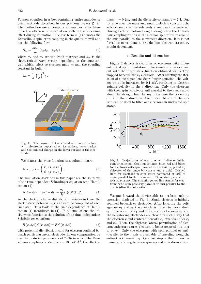
The proposed nanodevice is based on the planar het-erostructure described in the previous paper [6]. Its ver-tical cross-section is depicted in Fig. 1. The nanostruc-
ture consists of a quantum well 10 nm high sandwichedbetween two tunnel barriers of the same height. Thequantum well is separated from strongly doped substrateby 50 nm thick dopant-free buffer. Metal electrodes aredeposited on top of the upper barrier. If one places, in thequantum well, an electron forming a charge cloud, it willinduce an opposite charge on the surface of the conductorabove. The induced charge attracts the electron and theelectric field has a component directed to the center ofthe cloud. The self-focusing effect of the wave functionoccurs [8]. As the result the electron is trapped beneaththe metal electrode forming a stable wave packet, whichexhibits finite spatial extent and conserves its shape asit travels along the path determined by the electrode [9].Such wave packet shows features unique for a quantumparticle to have, as it reflects from a potential barrier ortunnels through it with probability of 1 like a classical ob-ject. This fact makes it possible to transfer the electronbetween different sites of the nanodevice in a controllablemanner.
3. Model
Despite its classical behavior the electron time evolu-tion is described in the framework of quantum mechanicsusing time-dependent Schrödinger equation. We also de-scribe electron spin quantum mechanically. The electronis set in motion by voltages applied to the electrodes.We choose the coordinates x and z in the quantum wellplane and y pointed in the direction of layer growth. Themotion in the y direction is forbidden due to trapping inthe quantum well. In the description of the motion inthe (x, z) plane we use the following Hamiltonian:
H (x, z, t) = − ~2
2m
(∂2
∂x2+
∂2
∂z2
)
− eϕ (x, y0, z, t) +HD , (1)
where y0 denotes the center of the quantum well, ϕ(r, t) isthe electrostatic potential being the result of solving the
(651)
652 P. Szumniak et al.
Poisson equation in a box containing entire nanodeviceusing methods described in our previous papers [5, 8].The method we use in computation enables us to deter-mine the electron time evolution with the self-focusingeffect during its motion. The last term in (1) denotes theDresselhaus spin–orbit coupling in the quantum well andhas the following form:
HD =~ksom
(pxσx − pzσz) , (2)
where σx and σz are the Pauli matrices and kso is thecharacteristic wave vector dependent on the quantumwell width, effective electron mass m and the couplingconstant in bulk γ:
kso =m
~
(πd
)2
γ .
Fig. 1. The layout of the considered nanostructurewith electrodes deposited on its surface, wave packetand the induced charge on the lower surface of the elec-trode.
We denote the wave function as a column matrix
Ψ(x, z, t) =
(ψ1 (x, z, t)
ψ2 (x, z, t)
). (3)
The simulation described in this paper are the solutionsof the time-dependent Schrödinger equation with Hamil-tonian (1):
Ψ(t+ dt) = Ψ(t− dt)− 2i
~H(t)Ψ(t)dt . (4)
As the electron charge distribution variates in time, theelectrostatic potential ϕ(r, t) has to be computed at eachtime step. This leads to the time dependence of Hamil-tonian (1) introduced in (4). In all simulations the ini-tial wave function is the solution of the time-independentSchrödinger equation:
H(x, z, 0)Ψ(x, z, 0) = EΨ(x, z, 0) (5)
with potential distribution valid for electron confined be-neath particular metal electrode. In our computation weuse the material parameters of ZnTe in which the Dres-selhaus coupling constant is γ = 13.3 eV Å3, the effective
mass m = 0.2me and the dielectric constant ε = 7.4. Dueto large effective mass and small dielectric constant, theself-focusing effect is relatively strong in this material.During electron motion along a straight line the Dressel-haus coupling results in the electron spin rotation aroundthe axis parallel to the movement direction. If it is notforced to move along a straight line, electron trajectoryis spin-dependent.
4. Results and discussion
Figure 2 depicts trajectories of electrons with differ-ent initial spin orientation. The simulation was carriedout with the initial wave function obtained for electrontrapped beneath the e1 electrode. After starting the iter-ation of time-dependent Schrödinger equation, the volt-age on e2 is increased by 0.1 mV, resulting in electrongaining velocity in the z direction. Only the electronswith their spin parallel or anti-parallel to the z axis movealong the straight line. In any other case the trajectorydrifts in the x direction. Such perturbation of the mo-tion can be used to filter out electrons in undesired spinstates.
Fig. 2. Trajectories of electrons with diverse initialspin orientation. Continuous lines: blue, red and blackfor electrons with spin parallel to the axis: x, y and xy(bisector of the angle between x and y axis). Dashedlines for electrons in spin states composed of 90% ofstate parallel to the z axis and 10% of state parallel toaxis x, y or xy. The straight yellow line stands for elec-trons with spin precisely parallel or anti-parallel to thez axis (direction of motion).
We put forward the device able to perform such anoperation depicted in Fig. 3. Single electron is initiallyconfined beneath e1 electrode. After lowering the volt-ages on e1 and e2 the particle is forced to move alonge3. The width of e3 and the distances between e3 andthe neighboring electrodes are chosen in such a way thatthe electron cloud centered beneath e3 extends under e4and e5. Then, the slightest lateral perturbation of elec-tron trajectory causes electron to be intercepted by eithere4 or e5. Only the electrons with spin parallel or anti--parallel to the z axis are capable of traveling along theentire track beneath e6. One last step of the process re-maining is telling between spin up and spin down states.
Nanodevice for High Precision Readout of Electron Spin 653
Fig. 3. The layout of electrodes in a nanodevicefiltering-out electrons in spin state having any x or ycomponent. The trajectories of electrons with differentspins are marked as in Fig. 2. The area marked withvertical lines contains the semimagnetic semiconductorand is used to distinguish between spin parallel to z axisfrom anti-parallel one.
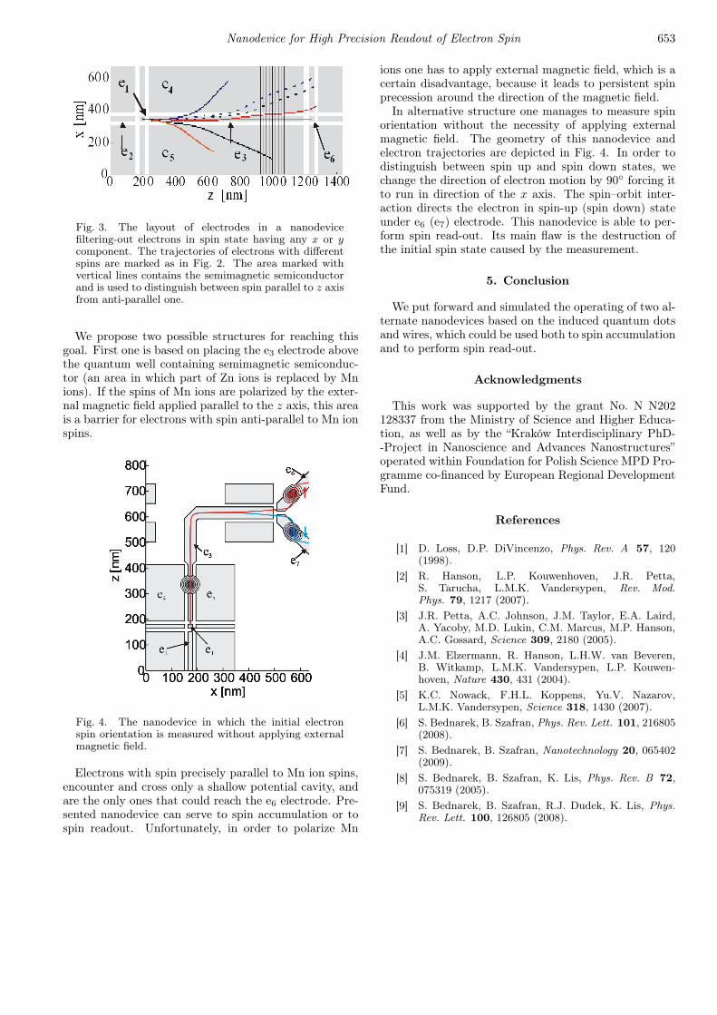
We propose two possible structures for reaching thisgoal. First one is based on placing the e3 electrode abovethe quantum well containing semimagnetic semiconduc-tor (an area in which part of Zn ions is replaced by Mnions). If the spins of Mn ions are polarized by the exter-nal magnetic field applied parallel to the z axis, this areais a barrier for electrons with spin anti-parallel to Mn ionspins.
Fig. 4. The nanodevice in which the initial electronspin orientation is measured without applying externalmagnetic field.
Electrons with spin precisely parallel to Mn ion spins,encounter and cross only a shallow potential cavity, andare the only ones that could reach the e6 electrode. Pre-sented nanodevice can serve to spin accumulation or tospin readout. Unfortunately, in order to polarize Mn
ions one has to apply external magnetic field, which is acertain disadvantage, because it leads to persistent spinprecession around the direction of the magnetic field.
In alternative structure one manages to measure spinorientation without the necessity of applying externalmagnetic field. The geometry of this nanodevice andelectron trajectories are depicted in Fig. 4. In order todistinguish between spin up and spin down states, wechange the direction of electron motion by 90◦ forcing itto run in direction of the x axis. The spin–orbit inter-action directs the electron in spin-up (spin down) stateunder e6 (e7) electrode. This nanodevice is able to per-form spin read-out. Its main flaw is the destruction ofthe initial spin state caused by the measurement.
5. Conclusion
We put forward and simulated the operating of two al-ternate nanodevices based on the induced quantum dotsand wires, which could be used both to spin accumulationand to perform spin read-out.
Acknowledgments
This work was supported by the grant No. N N202128337 from the Ministry of Science and Higher Educa-tion, as well as by the “Kraków Interdisciplinary PhD--Project in Nanoscience and Advances Nanostructures”operated within Foundation for Polish Science MPD Pro-gramme co-financed by European Regional DevelopmentFund.
References
[1] D. Loss, D.P. DiVincenzo, Phys. Rev. A 57, 120(1998).
[2] R. Hanson, L.P. Kouwenhoven, J.R. Petta,S. Tarucha, L.M.K. Vandersypen, Rev. Mod.Phys. 79, 1217 (2007).
[3] J.R. Petta, A.C. Johnson, J.M. Taylor, E.A. Laird,A. Yacoby, M.D. Lukin, C.M. Marcus, M.P. Hanson,A.C. Gossard, Science 309, 2180 (2005).
[4] J.M. Elzermann, R. Hanson, L.H.W. van Beveren,B. Witkamp, L.M.K. Vandersypen, L.P. Kouwen-hoven, Nature 430, 431 (2004).
[5] K.C. Nowack, F.H.L. Koppens, Yu.V. Nazarov,L.M.K. Vandersypen, Science 318, 1430 (2007).
[6] S. Bednarek, B. Szafran, Phys. Rev. Lett. 101, 216805(2008).
[7] S. Bednarek, B. Szafran, Nanotechnology 20, 065402(2009).
[8] S. Bednarek, B. Szafran, K. Lis, Phys. Rev. B 72,075319 (2005).
[9] S. Bednarek, B. Szafran, R.J. Dudek, K. Lis, Phys.Rev. Lett. 100, 126805 (2008).
4 SPIN ACCUMULATION AND SPIN READ OUT WITHOUT MAGNETIC FIELD
4 Spin accumulation and spin read out without mag-
netic field
22
Spin accumulation and spin read out without magnetic field
S. Bednarek, P. Szumniak, and B. SzafranFaculty of Physics and Applied Computer Science, AGH University of Science and Technology, al. Mickiewicza 30, 30-059
Kraków, Poland�Received 21 October 2010; published 16 December 2010�
An idea for construction of two spintronic single-electron nanodevices is presented and supported by aquantum-mechanical simulation of their operation. The first device selects electrons of a given spin orientationand the other performs the spin read out. The operation of proposed devices exploits the spin-dependentdeflection of electron trajectories induced by the spin-orbit Rashba coupling and does not require application ofan external magnetic field. The operation of the nanodevice requires application of weak voltages applied to theelectrodes only.
DOI: 10.1103/PhysRevB.82.235319 PACS number�s�: 73.63.Nm, 72.25.�b, 03.67.Lx
I. INTRODUCTION
Many extensive efforts have been conducted for fabrica-tion of a quantum computer based on the semiconductornanostructures. The quantum bit of information is supposedto be stored in the electron spin confined in a quantum dot.1–3
Electrostatic quantum dots4–8 are considered particularlypromising for quantum logic processing including the stor-age of single separate electrons and operations on their spins.In most of the devices constructed so far the modification ofthe electron spin state is induced by absorption of microwaveradiation in high magnetic field that energetically separatesthe spin-up and spin-down states. This is the most directmethod for rotation of a single-electron spin. However, themicrowave radiation is not suitable for addressing a singlespin in a register of several qubits contained within the samenanostructure. The use of the external microwave radiationwas avoided in a device of Ref. 8 in which the spin rotationis accomplished due to the spin-orbit �SO� coupling. Thisdevice8 still requires application of an external magneticfield, which induces a continuous precession of spins of allthe confined electrons. The inhomogeneities of this field re-sult in dephasing of the precession of separate spins. A de-vice that could operate without an external magnetic fieldwould be free of this source of decoherence. Recently, weproposed a couple of devices rotating the electron spins with-out the external magnetic field.9,10 We introduced an idea andsimulated the operation of nanodevices that perform thesingle-qubit Haddamard, negation and phase change quan-tum gate operations. The nanodevices exploit the self-focusing of electron wave function due to interaction withthe electron gas of the electrodes.11 The interaction allowsfor formation of a stable electron wave packet that can be putin motion by low voltages applied to the electrodes. Themotion of the electron along any desired trajectory combinedwith the spin-orbit coupling allows for arbitrary spin rota-tions. In this work we present an idea for construction of spinfilters that do without the external magnetic field. A firstvariant of the nanodevice can be used for selection of anelectron of a desired spin orientation for the purpose of theinitial state set up. The second variant is suitable for the spinread out on the final state.
II. DEVICE AND NUMERICAL METHOD
The proposed device is based on a planar heterostructuresimilar to the one previously used in Ref. 9 with a schematiccross section given in Fig. 1. The nanostructure contains aquantum well 10 nm wide sandwiched between two barrierseach of 10 nm width. The quantum well is separated from thesubstrate by a 50 nm thick undoped layer. On top of theupper blocking layer the metal electrodes are deposited.Electron confined in the quantum well forms a charge“cloud” distribution that induces an appearance of positivecharge on the lower surface of the metal electrodes. Theelectric field stemming from the positive induced charge pos-sesses an in-plane component directed to the center of theelectron charge distribution. The wave function of the elec-tron that is formed in this way becomes a stable packet thatcan move within the quantum well with a constant shape.When the self-focusing effect is strong enough �the quantumwell is close to the electrodes and the dielectric constant isnot too large� the scattering properties of the wave packetbecome classical, i.e., the electron backscatters or transfersthrough a potential defect with a 0% or 100% probability.11
The electron with classical scattering properties is still de-scribed by the time-dependent Schrödinger equation. Theelectron spin is also described in a standard way as two-row
Inducedcharge
x
zy
substrate
blocking barrier
blocking barrier
quantum well
Electron
FIG. 1. �Color online� Schematics of the considered nanodevicewith electrodes deposited on top, the electron wave packet, and thecharge induced on the lower surface of the electrode.
PHYSICAL REVIEW B 82, 235319 �2010�
1098-0121/2010/82�23�/235319�5� ©2010 The American Physical Society235319-1
single-column vectors. We choose the system of coordinatesin which the y axis is oriented parallel to the growth direc-tion. The electron motion in this direction is frozen. Theelectron is free to move in the x and z directions within thequantum well. Its wave function
��x,z,t� = ��1�x,z,t��2�x,z,t�
� �1�
depends on two spatial coordinates and time. The time de-pendence is described by the Schrödinger equation
��x,z,t + dt� = ��x,z,t − dt� −2i
�H��x,z,t�dt �2�
with Hamiltonian
H�x,z,t� = −�2
2m� �2
�x2 +�2
�z2� − e��x,y0,z,t� + HR, �3�
where y0 is the center of the quantum well and ��x ,y0 ,z , t� isthe electrostatic potential due to the electrodes and thecharges induced on them. The potential is found by solutionof the Poisson equation in a three-dimensional box that con-tains the entire nanodevice. The Poisson equation needs to besolved in every time step due to the motion of the wavepacket. The description of the method is given in Refs. 9 and12. The Poisson equation gives the classical potential distri-bution. Quantum calculations13 indicate that this is a goodapproximation of the actual response potential of the electrongas. The applied approach allows correctly describes theself-focusing mechanism and allows for investigation of themotion of the electron packet. The last term of Hamiltonian�3� accounts for the Rashba spin-orbit interaction14
HR = ��pz�x − px�z� , �4�
where p’s are the momentum operators and �’s are the Paulimatrices. In the initial moment of each simulation the wavefunction was assumed as a solution to the time-independentSchrödinger equation with the electron cloud distributioncorresponding to the bound state confined under one of theelectrodes,
H�x,z,0���x,z,0� = E��x,z,0� . �5�
In the calculations we adopted Si material parameters withm=0.19m0, the dielectric constant �=13, and the Rashbacoupling constant �=7.2�10−13 eV m.
III. RESULTS AND DISCUSSION
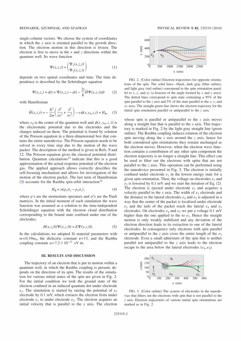
The trajectory of an electron that is put in motion within aquantum well, in which the Rashba coupling is present, de-pends on the direction of its spin. The results of the simula-tion for various initial states of the spin are given in Fig. 2.For the initial condition we took the ground state of theelectron confined in an induced quantum dot under electrodee1. The simulation is started by raising the potential of e2electrode by 0.1 mV, which extracts the electron from underelectrode e1 to under electrode e2. The electron acquires aninitial velocity that is parallel to the x axis. The electron
whose spin is parallel or antiparallel to the z axis movesalong a straight line that is parallel to the x axis. This trajec-tory is marked in Fig. 2 by the light gray straight line �greenonline�. The Rashba coupling induces rotation of the electronspin moving along the x axis around the z axis, hence forboth considered spin orientations they remain unchanged asthe electron moves. However, when the electron wave func-tion contains a contribution of any other spin component theelectron trajectory is no longer a straight line. This effect canbe used to filter out the electrons with spins that are notparallel to the z axis. This operation can be performed usingthe nanodevice presented in Fig. 3. The electron is initiallyconfined under electrode e1 in the lowest energy state for agiven spin orientation. Then, the voltage on electrodes e1 ande2 is lowered by 0.1 mV and we start the iteration of Eq. �2�.The electron is ejected under electrode e3 and acquires avelocity parallel to the x axis. The width of e3 electrode andthe distance to the lateral electrodes e4 and e5 is adjusted in away that the center of the packet is localized under electrodee3 and the tails of the packet reach the lateral e4 and e5electrodes. On electrodes e4 and e5 we put a voltage 0.1 mVhigher than the one applied to the to e3. Hence the straightmotion is only weakly stabilized and any deviation of theelectron direction leads to its extraction to one of the lateralelectrodes. In consequence only electrons with spin parallelor antiparallel to the z axis cross the entire length of the e3electrode. Even a small admixture of the spin that is neitherparallel not antiparallel to the z axis leads to the electronescape to the area below the lateral electrodes �e4 ,e5�.
0 500 1000 1500 2000 2500
x (nm)
0
200
400
600
z(n
m)
e e1 2
FIG. 2. �Color online� Electron trajectories for opposite orienta-tions of the spin. The solid lines—black, dark gray �blue online�,and light gray �red online� correspond to the spin orientation paral-lel to x, y, and xy �a bisector of the angle formed by x and y axes�.The dotted lines correspond to spin state containing a 95% of thespin parallel to the z axis and 5% of the state parallel to the x, y, andxy axes. The straight green line shows the electron trajectory for theinitial spin orientation parallel or antiparallel to the z axis.
0 100 200 300 400 500 600
x (nm)
0
50
100
150
200
z(n
m)
e
1
2 3
4
5
e e
e e
FIG. 3. �Color online� The system of electrodes in the nanode-vice that filters out the electrons with spin that is not parallel to thez axis. Electron trajectories of various initial spin orientations aremarked as in Fig. 2.
BEDNAREK, SZUMNIAK, AND SZAFRAN PHYSICAL REVIEW B 82, 235319 �2010�
235319-2
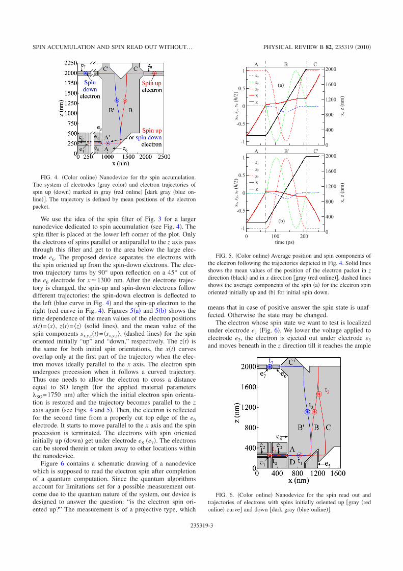
We use the idea of the spin filter of Fig. 3 for a largernanodevice dedicated to spin accumulation �see Fig. 4�. Thespin filter is placed at the lower left corner of the plot. Onlythe electrons of spins parallel or antiparallel to the z axis passthrough this filter and get to the area below the large elec-trode e6. The proposed device separates the electrons withthe spin oriented up from the spin-down electrons. The elec-tron trajectory turns by 90° upon reflection on a 45° cut ofthe e6 electrode for x�1300 nm. After the electrons trajec-tory is changed, the spin-up and spin-down electrons followdifferent trajectories: the spin-down electron is deflected tothe left �blue curve in Fig. 4� and the spin-up electron to theright �red curve in Fig. 4�. Figures 5�a� and 5�b� shows thetime dependence of the mean values of the electron positionsx�t�= �x�, z�t�= �z� �solid lines�, and the mean value of thespin components sx,y,z�t�= �sx,y,z�. �dashed lines� for the spinoriented initially “up” and “down,” respectively. The z�t� isthe same for both initial spin orientations, the x�t� curvesoverlap only at the first part of the trajectory when the elec-tron moves ideally parallel to the x axis. The electron spinundergoes precession when it follows a curved trajectory.Thus one needs to allow the electron to cross a distanceequal to SO length �for the applied material parametersSO=1750 nm� after which the initial electron spin orienta-tion is restored and the trajectory becomes parallel to the zaxis again �see Figs. 4 and 5�. Then, the electron is reflectedfor the second time from a properly cut top edge of the e6electrode. It starts to move parallel to the x axis and the spinprecession is terminated. The electrons with spin orientedinitially up �down� get under electrode e8 �e7�. The electronscan be stored therein or taken away to other locations withinthe nanodevice.
Figure 6 contains a schematic drawing of a nanodevicewhich is supposed to read the electron spin after completionof a quantum computation. Since the quantum algorithmsaccount for limitations set for a possible measurement out-come due to the quantum nature of the system, our device isdesigned to answer the question: “is the electron spin ori-ented up?” The measurement is of a projective type, which
means that in case of positive answer the spin state is unaf-fected. Otherwise the state may be changed.
The electron whose spin state we want to test is localizedunder electrode e1 �Fig. 6�. We lower the voltage applied toelectrode e2, the electron is ejected out under electrode e3and moves beneath in the z direction till it reaches the ample
FIG. 4. �Color online� Nanodevice for the spin accumulation.The system of electrodes �gray color� and electron trajectories ofspin up �down� marked in gray �red online� �dark gray �blue on-line�. The trajectory is defined by mean positions of the electronpacket.
xz
0
400
800
1200
1600
2000
x,z(nm)
-1
-0.5
0
0.5
1
s x,sy,s z(h/2)
sxsysz
A B C
(a)
xz
0
400
800
1200
1600
2000
x,z(nm)
0 100 200time (ps)
-1
-0.5
0
0.5
1
s x,sy,s z(h/2)
sxsysz
A B' C'
(b)
FIG. 5. �Color online� Average position and spin components ofthe electron following the trajectories depicted in Fig. 4. Solid linesshows the mean values of the position of the electron packet in zdirection �black� and in x direction �gray �red online�, dashed linesshows the average components of the spin �a� for the electron spinoriented initially up and �b� for initial spin down.
FIG. 6. �Color online� Nanodevice for the spin read out andtrajectories of electrons with spins initially oriented up �gray �redonline� curve and down �dark gray �blue online�.
SPIN ACCUMULATION AND SPIN READ OUT WITHOUT… PHYSICAL REVIEW B 82, 235319 �2010�
235319-3
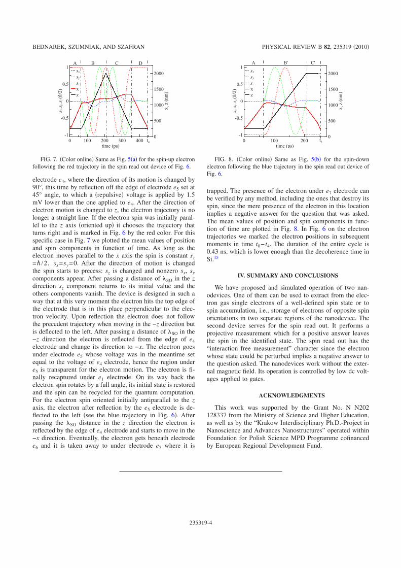
electrode e4, where the direction of its motion is changed by90°, this time by reflection off the edge of electrode e5 set at45° angle, to which a �repulsive� voltage is applied by 1.5mV lower than the one applied to e4. After the direction ofelectron motion is changed to z, the electron trajectory is nolonger a straight line. If the electron spin was initially paral-lel to the z axis �oriented up� it chooses the trajectory thatturns right and is marked in Fig. 6 by the red color. For thisspecific case in Fig. 7 we plotted the mean values of positionand spin components in function of time. As long as theelectron moves parallel to the x axis the spin is constant sz=� /2, sx=sy =0. After the direction of motion is changedthe spin starts to precess: sz is changed and nonzero sx, sycomponents appear. After passing a distance of SO in the zdirection sz component returns to its initial value and theothers components vanish. The device is designed in such away that at this very moment the electron hits the top edge ofthe electrode that is in this place perpendicular to the elec-tron velocity. Upon reflection the electron does not followthe precedent trajectory when moving in the −z direction butis deflected to the left. After passing a distance of SO in the−z direction the electron is reflected from the edge of e4electrode and change its direction to −x. The electron goesunder electrode e5 whose voltage was in the meantime setequal to the voltage of e4 electrode, hence the region undere5 is transparent for the electron motion. The electron is fi-nally recaptured under e1 electrode. On its way back theelectron spin rotates by a full angle, its initial state is restoredand the spin can be recycled for the quantum computation.For the electron spin oriented initially antiparallel to the zaxis, the electron after reflection by the e5 electrode is de-flected to the left �see the blue trajectory in Fig. 6�. Afterpassing the SO distance in the z direction the electron isreflected by the edge of e4 electrode and starts to move in the−x direction. Eventually, the electron gets beneath electrodee6 and it is taken away to under electrode e7 where it is
trapped. The presence of the electron under e7 electrode canbe verified by any method, including the ones that destroy itsspin, since the mere presence of the electron in this locationimplies a negative answer for the question that was asked.The mean values of position and spin components in func-tion of time are plotted in Fig. 8. In Fig. 6 on the electrontrajectories we marked the electron positions in subsequentmoments in time t0− t4. The duration of the entire cycle is0.43 ns, which is lower enough than the decoherence time inSi.15
IV. SUMMARY AND CONCLUSIONS
We have proposed and simulated operation of two nan-odevices. One of them can be used to extract from the elec-tron gas single electrons of a well-defined spin state or tospin accumulation, i.e., storage of electrons of opposite spinorientations in two separate regions of the nanodevice. Thesecond device serves for the spin read out. It performs aprojective measurement which for a positive answer leavesthe spin in the identified state. The spin read out has the“interaction free measurement” character since the electronwhose state could be perturbed implies a negative answer tothe question asked. The nanodevices work without the exter-nal magnetic field. Its operation is controlled by low dc volt-ages applied to gates.
ACKNOWLEDGMENTS
This work was supported by the Grant No. N N202128337 from the Ministry of Science and Higher Education,as well as by the “Krakow Interdisciplinary Ph.D.-Project inNanoscience and Advances Nanostructures” operated withinFoundation for Polish Science MPD Programme cofinancedby European Regional Development Fund.
xz
0
500
1000
1500
2000
x ,z(nm)
0 100 200 300 400time (ps)
-1
-0.5
0
0.5
1s x,sy,s z(h/2)
sxsysz
A B C D
t4
FIG. 7. �Color online� Same as Fig. 5�a� for the spin-up electronfollowing the red trajectory in the spin read out device of Fig. 6.
xz
0
500
1000
1500
2000
x ,z(nm)
0 100 200time (ps)
-1
-0.5
0
0.5
1
s x,sy,s z(h/2)
sxsysz
t3
A B' C'
FIG. 8. �Color online� Same as Fig. 5�b� for the spin-downelectron following the blue trajectory in the spin read out device ofFig. 6.
BEDNAREK, SZUMNIAK, AND SZAFRAN PHYSICAL REVIEW B 82, 235319 �2010�
235319-4
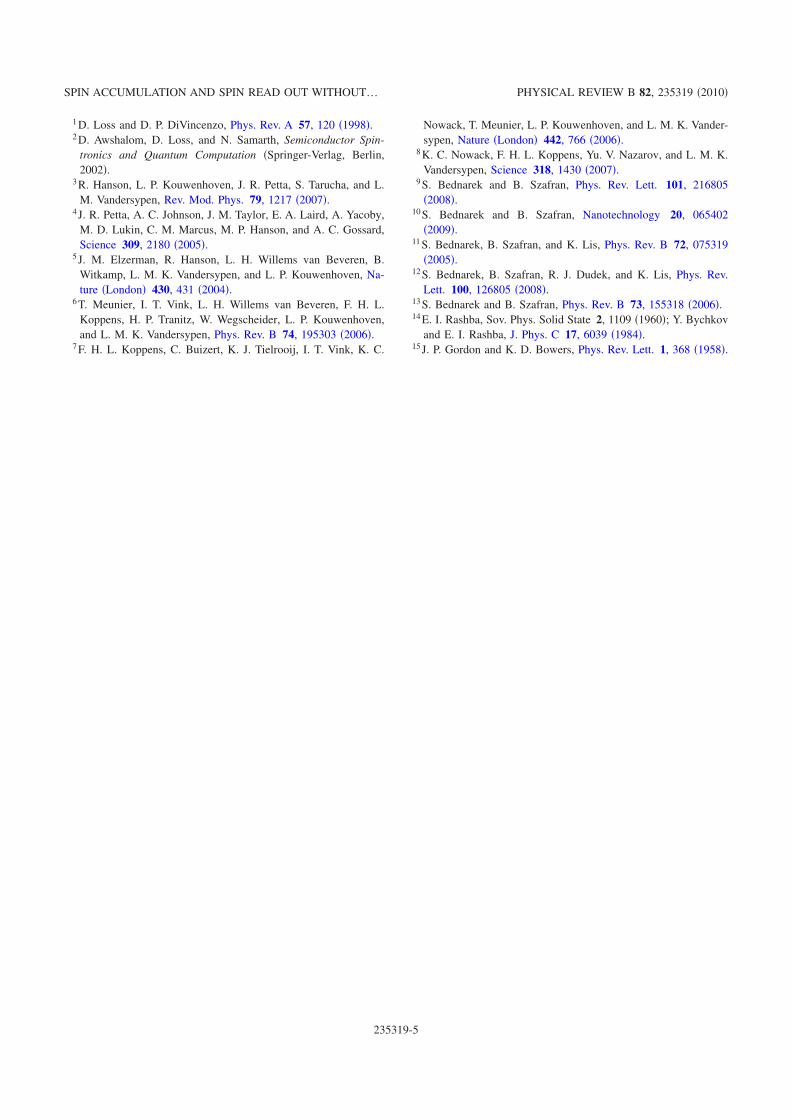
1 D. Loss and D. P. DiVincenzo, Phys. Rev. A 57, 120 �1998�.2 D. Awshalom, D. Loss, and N. Samarth, Semiconductor Spin-
tronics and Quantum Computation �Springer-Verlag, Berlin,2002�.
3 R. Hanson, L. P. Kouwenhoven, J. R. Petta, S. Tarucha, and L.M. Vandersypen, Rev. Mod. Phys. 79, 1217 �2007�.
4 J. R. Petta, A. C. Johnson, J. M. Taylor, E. A. Laird, A. Yacoby,M. D. Lukin, C. M. Marcus, M. P. Hanson, and A. C. Gossard,Science 309, 2180 �2005�.
5 J. M. Elzerman, R. Hanson, L. H. Willems van Beveren, B.Witkamp, L. M. K. Vandersypen, and L. P. Kouwenhoven, Na-ture �London� 430, 431 �2004�.
6 T. Meunier, I. T. Vink, L. H. Willems van Beveren, F. H. L.Koppens, H. P. Tranitz, W. Wegscheider, L. P. Kouwenhoven,and L. M. K. Vandersypen, Phys. Rev. B 74, 195303 �2006�.
7 F. H. L. Koppens, C. Buizert, K. J. Tielrooij, I. T. Vink, K. C.
Nowack, T. Meunier, L. P. Kouwenhoven, and L. M. K. Vander-sypen, Nature �London� 442, 766 �2006�.
8 K. C. Nowack, F. H. L. Koppens, Yu. V. Nazarov, and L. M. K.Vandersypen, Science 318, 1430 �2007�.
9 S. Bednarek and B. Szafran, Phys. Rev. Lett. 101, 216805�2008�.
10 S. Bednarek and B. Szafran, Nanotechnology 20, 065402�2009�.
11 S. Bednarek, B. Szafran, and K. Lis, Phys. Rev. B 72, 075319�2005�.
12 S. Bednarek, B. Szafran, R. J. Dudek, and K. Lis, Phys. Rev.Lett. 100, 126805 �2008�.
13 S. Bednarek and B. Szafran, Phys. Rev. B 73, 155318 �2006�.14 E. I. Rashba, Sov. Phys. Solid State 2, 1109 �1960�; Y. Bychkov
and E. I. Rashba, J. Phys. C 17, 6039 �1984�.15 J. P. Gordon and K. D. Bowers, Phys. Rev. Lett. 1, 368 �1958�.
SPIN ACCUMULATION AND SPIN READ OUT WITHOUT… PHYSICAL REVIEW B 82, 235319 �2010�
235319-5
5 SPIN-ORBIT-MEDIATED MANIPULATION OF HEAVY-HOLE SPIN QUBITSIN GATED SEMICONDUCTOR NANODEVICES
5 Spin-Orbit-Mediated Manipulation of Heavy-Hole
Spin Qubits in Gated Semiconductor Nanodevices
28
Spin-Orbit-Mediated Manipulation of Heavy-Hole Spin Qubitsin Gated Semiconductor Nanodevices
P. Szumniak,1,2 S. Bednarek,1 B. Partoens,2 and F.M. Peeters2
1Faculty of Physics and Applied Computer Science, AGH University of Science and Technology,al. Mickiewicza 30, 30-059 Krakow, Poland
2Departement Fysica, Universiteit Antwerpen, Groenenborgerlaan 171, B-2020 Antwerpen, Belgium(Received 10 February 2012; published 4 September 2012)
A novel spintronic nanodevice is proposed that is able to manipulate the single heavy-hole spin state in a
coherentmanner. It can act as a single quantum logic gate. The heavy-hole spin transformations are realized by
transporting thehole aroundclosed loops definedbymetal gates depositedon topof thenanodevice.Thedevice
exploitsDresselhaus spin-orbit interaction,which translates the spatial motion of the hole into a rotation of the
spin. The proposed quantumgate operates on subnanosecond time scales and requires only the application of a
weak static voltagewhich allows for addressing heavy-hole spin qubits individually. Our results are supported
by quantum mechanical time-dependent calculations within the four-band Luttinger-Kohn model.
DOI: 10.1103/PhysRevLett.109.107201 PACS numbers: 75.76.+j, 03.67.Lx, 71.70.Ej, 85.75.�d
There is currently great interest in studying spin relatedphenomena in semiconductors. On the one hand there isnovel fundamental physics at the nanoscale and on theother hand one expects applications in terms of spin basedquantum information processing [1,2]. Physical realizationof quantum computers requires fulfillment of a number ofchallenging criteria [3]. A fragile quantum state has to becoherent for sufficient long time which usually requires itsisolation from the environment. On the other hand it has tobe externally manipulated. For these purposes, the electronspin in semiconductor quantum dots was suggested as apromising candidate [4]. There are a number of experi-ments in which the electron spin is initialized, manipu-lated, stored, and read out [5–11].
Usually spin-state manipulation requires the applicationof microwave radiation, radio-frequency electric fields aswell as magnetic fields. These methods strongly limits thepossibility to address spins qubits individually. The firststep towards selective control of individual single electronspins was demonstrated in recent state of the art experi-ments [12,13]. Electron spin manipulation was realized bymeans of electric fields which can be generated locallyquite easily and indirectly via spin orbit interaction whichcouples charge and spin degrees of freedom. Electron spincontrol based on spin orbit effect was also proposed insome theoretical papers [14–18].
Unfortunately, in most semiconductor quantum dots theelectron spin is exposed to hyperfine interaction with nu-clear spins which are present in the host material. Thisinteraction is then the main source of electron spin deco-herence in quantum dots putting a severe restriction on thepossibility to realize a highly coherent electron spin qubit[19,20]. There are several appealing ideas how to deal withthis type of decoherence in quantum dot systems [21]. Verypromising way to eliminate or reduce the contact hyperfineinteraction with the nuclear spin lattice is to use the spinstate of the valence holes—a missing electron in the
valence band—as a carrier of quantum information insteadof electrons. Holes are described by the p orbitals thatvanish at a nuclear site, which strongly suppresses theFermi hyperfine contact interaction. Thus one can expectlonger coherence times for hole spin states [22,23]. Someexperiments seem to confirm this statement reporting longrelaxation (�ms) and coherence (��s) times [24–27] forhole spins while others reported a very short hole spindephasing time (�ns) [28]. Recent theoretical investiga-tions [29,30] and experiments [31] seem to resolve thismismatch of coherence times in different experiments sug-gesting that the absence of mixing between the heavy-hole(HH) and the light-hole(LH) state is crucial for a long holespin coherence time. Not only long coherence times butalso the possibility to initialize the hole spin state evenwithout a magnetic field [25], and the recent realization of acoherent control of a hole spin state in single and doublecoupled quantum dots [32–34] has promoted the hole as avery good candidate as carrier of quantum bit information.There are also a few appealing theoretical proposals howthe HH spin state can be manipulated [35–39].In this Letter, we demonstrate by using a four-band HH-
LH model that the motion of the valence hole in gatedsemiconductor nanostructures can induce the rotation ofthe HH spin in the presence of the Dresselhaus spin-orbitinteraction (DSOI). Supported by these results we presentan efficient scheme which can be used to realize anyrotation of the HH spin and propose a nanodevice whichacts as a quantum logic NOT gate on a HH spin qubit. Thespin rotations are realized by transporting the hole alonga closed loop which is defined by metal gates. This methodis more suitable for controlling the hole spin than theapplication of a magnetic field, because the in-plane holeg factor is very small. Therefore, one would need a mag-netic field of several Teslas, which is still experimentallychallenging. Application of the multiband model allows usto study mixing between HH and LH states. We found that
PRL 109, 107201 (2012) P HY S I CA L R EV I EW LE T T E R Sweek ending
7 SEPTEMBER 2012
0031-9007=12=109(10)=107201(5) 107201-1 � 2012 American Physical Society
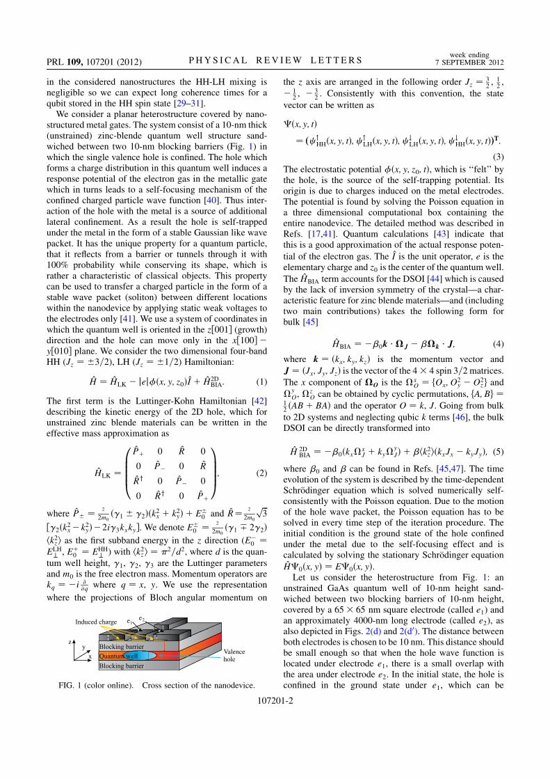
in the considered nanostructures the HH-LH mixing isnegligible so we can expect long coherence times for aqubit stored in the HH spin state [29–31].
We consider a planar heterostructure covered by nano-structured metal gates. The system consist of a 10-nm thick(unstrained) zinc-blende quantum well structure sand-wiched between two 10-nm blocking barriers (Fig. 1) inwhich the single valence hole is confined. The hole whichforms a charge distribution in this quantum well induces aresponse potential of the electron gas in the metallic gatewhich in turns leads to a self-focusing mechanism of theconfined charged particle wave function [40]. Thus inter-action of the hole with the metal is a source of additionallateral confinement. As a result the hole is self-trappedunder the metal in the form of a stable Gaussian like wavepacket. It has the unique property for a quantum particle,that it reflects from a barrier or tunnels through it with100% probability while conserving its shape, which israther a characteristic of classical objects. This propertycan be used to transfer a charged particle in the form of astable wave packet (soliton) between different locationswithin the nanodevice by applying static weak voltages tothe electrodes only [41]. We use a system of coordinates inwhich the quantum well is oriented in the z½001� (growth)direction and the hole can move only in the x½100� �y½010� plane. We consider the two dimensional four-bandHH (Jz ¼ �3=2), LH (Jz ¼ �1=2) Hamiltonian:
H ¼ HLK � jej�ðx; y; z0ÞI þ H2DBIA: (1)
The first term is the Luttinger-Kohn Hamiltonian [42]describing the kinetic energy of the 2D hole, which forunstrained zinc blende materials can be written in theeffective mass approximation as
HLK ¼
Pþ 0 R 0
0 P� 0 R
Ry 0 P� 0
0 Ry 0 Pþ
0BBBBB@
1CCCCCA; (2)
where P� ¼ 2
2m0ð�1 � �2Þðk2x þ k2yÞ þ E�
0 and R¼ 2
2m0
ffiffiffi3
p
½�2ðk2x�k2yÞ�2i�3kxky�. We denote E�0 ¼ 2
2m0ð�1 � 2�2Þ
hk2zi as the first subband energy in the z direction (E�0 ¼
ELH? , Eþ
0 ¼ EHH? ) with hk2zi ¼ �2=d2, where d is the quan-
tum well height, �1, �2, �3 are the Luttinger parametersand m0 is the free electron mass. Momentum operators arekq ¼ �i @
@q where q ¼ x, y. We use the representation
where the projections of Bloch angular momentum on
the z axis are arranged in the following order Jz ¼ 32 ,
12 ,� 1
2 , � 32 . Consistently with this convention, the state
vector can be written as
�ðx;y; tÞ¼ ðc "
HHðx;y; tÞ;c "LHðx;y; tÞ;c #
LHðx;y; tÞ;c #HHðx;y; tÞÞT:
(3)
The electrostatic potential �ðx; y; z0; tÞ, which is ‘‘felt’’ bythe hole, is the source of the self-trapping potential. Itsorigin is due to charges induced on the metal electrodes.The potential is found by solving the Poisson equation ina three dimensional computational box containing theentire nanodevice. The detailed method was described inRefs. [17,41]. Quantum calculations [43] indicate thatthis is a good approximation of the actual response poten-
tial of the electron gas. The I is the unit operator, e is theelementary charge and z0 is the center of the quantum well.
The HBIA term accounts for the DSOI [44] which is causedby the lack of inversion symmetry of the crystal—a char-acteristic feature for zinc blende materials—and (includingtwo main contributions) takes the following form forbulk [45]
HBIA ¼ ��0k ��J � ��k � J; (4)
where k ¼ ðkx; ky; kzÞ is the momentum vector and
J ¼ ðJx; Jy; JzÞ is the vector of the 4� 4 spin 3=2matrices.
The x component of �O is the �xO ¼ fOx;O
2y �O2
zg and�y
O, �zO can be obtained by cyclic permutations, fA; Bg ¼
12 ðABþ BAÞ and the operator O ¼ k, J. Going from bulk
to 2D systems and neglecting qubic k terms [46], the bulkDSOI can be directly transformed into
H 2DBIA ¼ ��0ðkx�x
J þ ky�yJÞ þ �hk2ziðkxJx � kyJyÞ; (5)
where �0 and � can be found in Refs. [45,47]. The timeevolution of the system is described by the time-dependentSchrodinger equation which is solved numerically self-consistently with the Poisson equation. Due to the motionof the hole wave packet, the Poisson equation has to besolved in every time step of the iteration procedure. Theinitial condition is the ground state of the hole confinedunder the metal due to the self-focusing effect and iscalculated by solving the stationary Schrodinger equation
H�0ðx; yÞ ¼ E�0ðx; yÞ.Let us consider the heterostructure from Fig. 1: an
unstrained GaAs quantum well of 10-nm height sand-wiched between two blocking barriers of 10-nm height,covered by a 65� 65 nm square electrode (called e1) andan approximately 4000-nm long electrode (called e2), asalso depicted in Figs. 2(d) and 2(d0). The distance betweenboth electrodes is chosen to be 10 nm. This distance shouldbe small enough so that when the hole wave function islocated under electrode e1, there is a small overlap withthe area under electrode e2. In the initial state, the hole isconfined in the ground state under e1, which can be
Valenceholex
yz
e e1
2
FIG. 1 (color online). Cross section of the nanodevice.
PRL 109, 107201 (2012) P HY S I CA L R EV I EW LE T T E R Sweek ending
7 SEPTEMBER 2012
107201-2
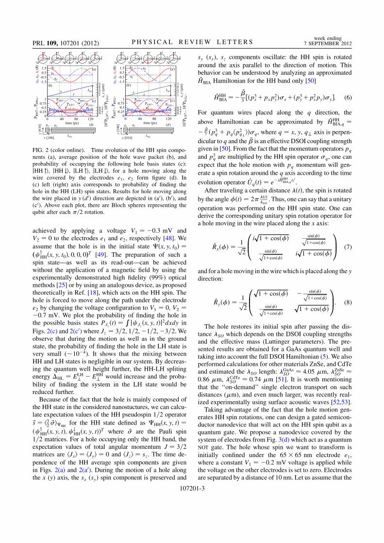
achieved by applying a voltage V1 ¼ �0:3 mV andV2 ¼ 0 to the electrodes e1 and e2, respectively [48]. We
assume that the hole is in the initial state �ðx; y; t0Þ ¼ðc "
HHðx; y; t0Þ; 0; 0; 0ÞT [49]. The preparation of such a
spin state—as well as its read-out—can be achievedwithout the application of a magnetic field by using theexperimentally demonstrated high fidelity (99%) opticalmethods [25] or by using an analogous device, as proposedtheoretically in Ref. [18], which acts on the HH spin. Thehole is forced to move along the path under the electrodee2 by changing the voltage configuration to V1 ¼ 0, V2 ¼�0:7 mV. We plot the probability of finding the hole inthe possible basis states PJzðtÞ ¼
R jc Jzðx; y; tÞj2dxdy in
Figs. 2(c) and 2(c0) where Jz ¼ 3=2, 1=2,�1=2,�3=2. Weobserve that during the motion as well as in the groundstate, the probability of finding the hole in the LH state isvery small (�10�4). It shows that the mixing betweenHH and LH states is negligible in our system. By decreas-ing the quantum well height further, the HH-LH splitingenergy �HL ¼ ELH
? � EHH? would increase and the proba-
bility of finding the system in the LH state would bereduced further.
Because of the fact that the hole is mainly composed ofthe HH state in the considered nanostuctures, we can calcu-late expectation values of the HH pseudospin 1=2 operator
~s ¼ h32 ~�i�HHfor the HH state defined as �HHðx; y; tÞ ¼
ðc "HHðx; y; tÞ; c #
HHðx; y; tÞÞT where ~� are the Pauli spin
1=2 matrices. For a hole occupying only the HH band, theexpectation values of total angular momentum J ¼ 3=2matrices are hJxi ¼ hJyi ¼ 0 and hJzi ¼ sz. The time de-
pendence of the HH average spin components are givenin Figs. 2(a) and 2(a0). During the motion of a hole alongthe x (y) axis, the sx (sy) spin component is preserved and
sy (sx), sz components oscillate: the HH spin is rotated
around the axis parallel to the direction of motion. Thisbehavior can be understood by analyzing an approximated
HBIA Hamiltonian for the HH band only [50]
HHHBIA¼�
~�3½ðp3
xþpxp2yÞ�xþðp3
yþp2xpyÞ�y�: (6)
For quantum wires placed along the q direction, the
above Hamiltonian can be approximated by HHHBIA;q ¼
� ~�3 ðp3
q þ pqhp2q?iÞ�q, where q ¼ x, y, q? axis is perpen-
dicular to q and the ~� is an effective DSOI coupling strengthgiven in [50]. From the fact that the momentum operatorspq
and p3q are multiplied by the HH spin operator �q, one can
expect that the hole motion with pq momentum will gen-
erate a spin rotation around the q axis according to the time
evolution operator UqðtÞ ¼ e�iHHHBIA;qt=.
After traveling a certain distance �ðtÞ, the spin is rotatedby the angle�ðtÞ ¼ 2� �ðtÞ
�SO. Thus, one can say that a unitary
operation was performed on the HH spin state. One canderive the corresponding unitary spin rotation operator fora hole moving in the wire placed along the x axis:
Rxð�Þ ¼ 1ffiffiffi2
piffiffiffiffiffiffiffiffiffiffiffiffiffiffiffiffiffiffiffiffiffiffiffi1þ cosð�Þp
sinð�Þffiffiffiffiffiffiffiffiffiffiffiffiffiffiffi1þcosð�Þ
psinð�Þffiffiffiffiffiffiffiffiffiffiffiffiffiffiffi1þcosð�Þ
p iffiffiffiffiffiffiffiffiffiffiffiffiffiffiffiffiffiffiffiffiffiffiffi1þ cosð�Þp
0BB@
1CCA (7)
and for a holemoving in thewirewhich is placed along the ydirection:
Ryð�Þ ¼ 1ffiffiffi2
pffiffiffiffiffiffiffiffiffiffiffiffiffiffiffiffiffiffiffiffiffiffiffi1þ cosð�Þp � sinð�Þffiffiffiffiffiffiffiffiffiffiffiffiffiffiffi
1þcosð�Þp
sinð�Þffiffiffiffiffiffiffiffiffiffiffiffiffiffiffi1þcosð�Þ
p ffiffiffiffiffiffiffiffiffiffiffiffiffiffiffiffiffiffiffiffiffiffiffi1þ cosð�Þp
0BB@
1CCA: (8)
The hole restores its initial spin after passing the dis-tance �SO which depends on the DSOI coupling strengthsand the effective mass (Luttinger parameters). The pre-sented results are obtained for a GaAs quantum well andtaking into account the full DSOI Hamiltonian (5). We alsoperformed calculations for other materials ZnSe, and CdTeand estimated the �SO length: �GaAs
SO � 4:05 �m, �ZnSeSO �
0:86 �m, �CdTeSO � 0:74 �m [51]. It is worth mentioning
that the ‘‘on-demand’’ single electron transport on suchdistances (�m), and even much larger, was recently real-ized experimentally using surface acoustic waves [52,53].Taking advantage of the fact that the hole motion gen-
erates HH spin rotations, one can design a gated semicon-ductor nanodevice that will act on the HH spin qubit as aquantum gate. We propose a nanodevice covered by thesystem of electrodes from Fig. 3(d) which act as a quantumNOT gate. The hole whose spin we want to transform is
initially confined under the 65� 65 nm electrode e1,where a constant V1 ¼ �0:2 mV voltage is applied whilethe voltage on the other electrodes is set to zero. Electrodesare separated by a distance of 10 nm. Let us assume that the
FIG. 2 (color online). Time evolution of the HH spin compo-nents (a), average position of the hole wave packet (b), andprobability of occupying the following hole basis states (c):jHH "i, jHH #i, jLH "i, jLH #i, for a hole moving along thewire covered by the electrodes e1, e2 form figure (d). In(c) left (right) axis corresponds to probability of finding thehole in the HH (LH) spin states. Results for hole moving alongthe wire placed in y ðd0Þ direction are depicted in (a0), (b0), and(c0). Above each plot, there are Bloch spheres representing thequbit after each �=2 rotation.
PRL 109, 107201 (2012) P HY S I CA L R EV I EW LE T T E R Sweek ending
7 SEPTEMBER 2012
107201-3
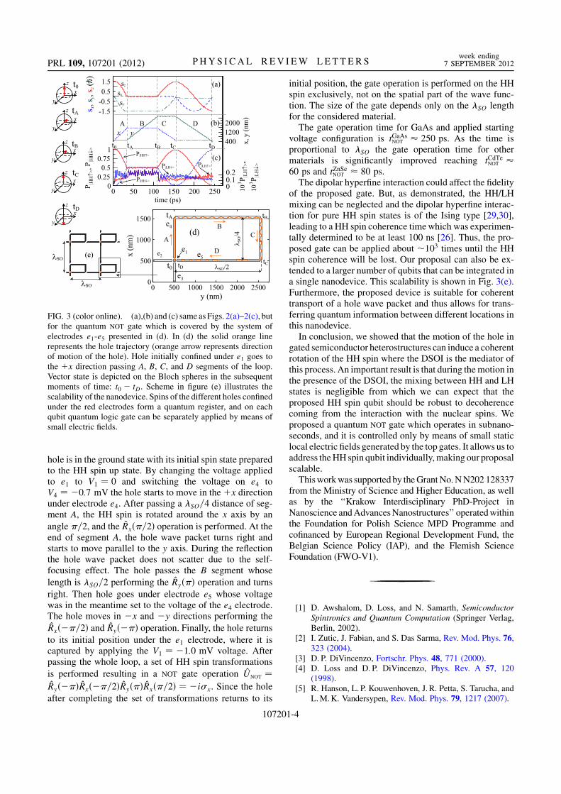
hole is in the ground state with its initial spin state preparedto the HH spin up state. By changing the voltage appliedto e1 to V1 ¼ 0 and switching the voltage on e4 toV4 ¼ �0:7 mV the hole starts to move in theþx directionunder electrode e4. After passing a �SO=4 distance of seg-ment A, the HH spin is rotated around the x axis by an
angle �=2, and the Rxð�=2Þ operation is performed. At theend of segment A, the hole wave packet turns right andstarts to move parallel to the y axis. During the reflectionthe hole wave packet does not scatter due to the self-focusing effect. The hole passes the B segment whose
length is �SO=2 performing the Ryð�Þ operation and turns
right. Then hole goes under electrode e5 whose voltagewas in the meantime set to the voltage of the e4 electrode.The hole moves in �x and �y directions performing the
Rxð��=2Þ and Ryð��Þ operation. Finally, the hole returnsto its initial position under the e1 electrode, where it iscaptured by applying the V1 ¼ �1:0 mV voltage. Afterpassing the whole loop, a set of HH spin transformations
is performed resulting in a NOT gate operation UNOT ¼Ryð��ÞRxð��=2ÞRyð�ÞRxð�=2Þ ¼ �i�x. Since the hole
after completing the set of transformations returns to its
initial position, the gate operation is performed on the HHspin exclusively, not on the spatial part of the wave func-tion. The size of the gate depends only on the �SO lengthfor the considered material.The gate operation time for GaAs and applied starting
voltage configuration is tGaAsNOT � 250 ps. As the time isproportional to �SO the gate operation time for othermaterials is significantly improved reaching tCdTeNOT �60 ps and tZnSeNOT � 80 ps.The dipolar hyperfine interaction could affect the fidelity
of the proposed gate. But, as demonstrated, the HH/LHmixing can be neglected and the dipolar hyperfine interac-tion for pure HH spin states is of the Ising type [29,30],leading to a HH spin coherence timewhich was experimen-tally determined to be at least 100 ns [26]. Thus, the pro-posed gate can be applied about �103 times until the HHspin coherence will be lost. Our proposal can also be ex-tended to a larger number of qubits that can be integrated ina single nanodevice. This scalability is shown in Fig. 3(e).Furthermore, the proposed device is suitable for coherenttransport of a hole wave packet and thus allows for trans-ferring quantum information between different locations inthis nanodevice.In conclusion, we showed that the motion of the hole in
gated semiconductor heterostructures can induce a coherentrotation of the HH spin where the DSOI is the mediator ofthis process. An important result is that during themotion inthe presence of the DSOI, the mixing between HH and LHstates is negligible from which we can expect that theproposed HH spin qubit should be robust to decoherencecoming from the interaction with the nuclear spins. Weproposed a quantum NOT gate which operates in subnano-seconds, and it is controlled only by means of small staticlocal electric fields generated by the top gates. It allows us toaddress theHHspin qubit individually,making our proposalscalable.Thisworkwas supported by theGrantNo.NN202 128337
from the Ministry of Science and Higher Education, as wellas by the ‘‘Krakow Interdisciplinary PhD-Project inNanoscience andAdvancesNanostructures’’ operatedwithinthe Foundation for Polish Science MPD Programme andcofinanced by European Regional Development Fund, theBelgian Science Policy (IAP), and the Flemish ScienceFoundation (FWO-V1).
[1] D. Awshalom, D. Loss, and N. Samarth, SemiconductorSpintronics and Quantum Computation (Springer Verlag,Berlin, 2002).
[2] I. Zutic, J. Fabian, and S. Das Sarma, Rev. Mod. Phys. 76,323 (2004).
[3] D. P. DiVincenzo, Fortschr. Phys. 48, 771 (2000).[4] D. Loss and D. P. DiVincenzo, Phys. Rev. A 57, 120
(1998).[5] R. Hanson, L. P. Kouwenhoven, J. R. Petta, S. Tarucha, and
L.M.K. Vandersypen, Rev. Mod. Phys. 79, 1217 (2007).
FIG. 3 (color online). (a),(b) and (c) same as Figs. 2(a)–2(c), butfor the quantum NOT gate which is covered by the system ofelectrodes e1-e5 presented in (d). In (d) the solid orange linerepresents the hole trajectory (orange arrow represents directionof motion of the hole). Hole initially confined under e1 goes tothe þx direction passing A, B, C, and D segments of the loop.Vector state is depicted on the Bloch spheres in the subsequentmoments of time: t0 � tD. Scheme in figure (e) illustrates thescalability of the nanodevice. Spins of the different holes confinedunder the red electrodes form a quantum register, and on eachqubit quantum logic gate can be separately applied by means ofsmall electric fields.
PRL 109, 107201 (2012) P HY S I CA L R EV I EW LE T T E R Sweek ending
7 SEPTEMBER 2012
107201-4
[6] S. Amasha, K. MacLean, I. P. Radu, D.M. Zumbuhl, M.A.Kastner, M. P. Hanson, and A. C. Gossard, Phys. Rev. Lett.100, 046803 (2008).
[7] J. R. Petta, A. C. Johnson, J.M. Taylor, E. A. Laird, A.Yacoby, M.D. Lukin, C.M. Marcus, M. P. Hanson, andA. C. Gossard, Science 309, 2180 (2005).
[8] J.M. Elzerman, R. Hanson, L. H. Willems van Beveren, B.Witkamp, L.M.K. Vandersypen, and L. P. Kouwenhoven,Nature (London) 430, 431 (2004).
[9] T. Meunier, I. T. Vink, L.H. Willems van Beveren, F.H.L.Koppens,H. P.Tranitz,W.Wegscheider,L. P.Kouwenhoven,and L.M.K. Vandersypen, Phys. Rev. B 74, 195303 (2006).
[10] F. H. L. Koppens, C. Buizert, K. J. Tielrooij, I. T. Vink,K. C. Nowack, T. Meunier, L. P. Kouwenhoven, andL.M.K. Vandersypen, Nature (London) 442, 766 (2006).
[11] A. Morello, J. J. Pla, F. A. Zwanenburg, K.W. Chan, K. Y.Tan, H. Huebl, M. Mottonen, C. D. Nugroho, C. Yang,J. A. van Donkelaar, A. D. C. Alves, D.N. Jamieson, C. C.Escott, L. C. L. Hollenberg, R. G. Clark, and A. S. Dzurak,Nature (London) 467, 687 (2010).
[12] K. C. Nowack, F. H. L. Koppens, Yu. V. Nazarov, andL.M.K. Vandersypen, Science 318, 1430 (2007).
[13] S. Nadj-Perge, S.M. Frolov, E. P. A.M. Bakkers, and L. P.Kouwenhoven, Nature (London) 468, 1084 (2010).
[14] V. N. Golovach, M. Borhani, and D. Loss, Phys. Rev. B 74,165319 (2006).
[15] S. Debald and C. Emary, Phys. Rev. Lett. 94, 226803 (2005).[16] C. Flindt, A. S. Sorensen, and K. Flensberg, Phys. Rev.
Lett. 97, 240501 (2006).[17] S. Bednarek and B. Szafran, Phys. Rev. Lett. 101, 216805
(2008).[18] S. Bednarek, P. Szumniak, and B. Szafran, Phys. Rev. B
82, 235319 (2010).[19] I. A. Merkulov, Al. L. Efros, and M. Rosen, Phys. Rev. B
65, 205309 (2002).[20] A. V. Khaetskii, D. Loss, and L. Glazman, Phys. Rev. Lett.
88, 186802 (2002).[21] J. Fischer and D. Loss, Science 324, 1277 (2009).[22] G. Burkard, Nature Mater. 7, 100 (2008).[23] M.H. Kolodrubetz and J. R. Petta, Science 325, 42 (2009).[24] D. Heiss, S. Schaeck, H. Huebl, M. Bichler, G. Abstreiter,
J. J. Finley, D. V. Bulaev, and D. Loss, Phys. Rev. B 76,241306 (2007).
[25] B. D. Gerardot, D. Brunner, P. A. Dalgarno, P. Ohberg, S.Seidl, M. Kroner, K. Karrai, N. G. Stoltz, P.M. Petroff,and R. J. Warburton, Nature (London) 451, 441 (2008).
[26] D. Brunner, B. D. Gerardot, P. A. Dalgarno, G. Wust, K.Karrai, N. G. Stoltz, P.M. Petroff, and R. J. Warburton,Science 325, 70 (2009).
[27] F. Fras, B. Eble, P. Desfonds, F. Bernardot, C. Testelin, M.Chamarro, A. Miard, and A. Lemaıtre, Phys. Rev. B 84,125431 (2011).
[28] B. Eble, C. Testelin, P. Desfonds, F. Bernardot, A.Balocchi, T. Amand, A. Miard, A. Lemaıtre, X. Marie,and M. Chamarro, Phys. Rev. Lett. 102, 146601 (2009).
[29] C. Testelin, F. Bernardot, B. Eble, and M. Chamarro, Phys.Rev. B 79, 195440 (2009).
[30] J. Fischer, W.A. Coish, D.V. Bulaev, and D. Loss, Phys.Rev. B 78, 155329 (2008).
[31] E. A. Chekhovich, A. B. Krysa, M. S. Skolnick, and A. I.Tartakovskii, Phys. Rev. Lett. 106, 027402 (2011).
[32] K. De Greve, P. L. McMahon, D. Press, T. D. Ladd, D.Bisping, C. Schneider, M. Kamp, L. Worschech, S.Hofling, A. Forchel, and Y. Yamamoto, Nature Phys. 7,872 (2011).
[33] A. Greilich, S. G. Carter, D. Kim, A. S. Bracker, and D.Gammon, Nature Photon. 5, 702 (2011).
[34] T.M. Godden, J. H. Quilter, A. J. Ramsay, Yanwen Wu, P.Brereton, S. J. Boyle, I. J. Luxmoore, J. Puebla-Nunez,A.M. Fox, and M. S. Skolnick, Phys. Rev. Lett. 108,017402 (2012).
[35] D. V. Bulaev and D. Loss, Phys. Rev. Lett. 98, 097202(2007).
[36] C. Y. Hsieh, R. Cheriton, M. Korkusinski, and P.Hawrylak, Phys. Rev. B 80, 235320 (2009).
[37] J. C. Budich, D.G. Rothe, E.M. Hankiewicz, and B.Trauzettel, Phys. Rev. B 85, 205425 (2012).
[38] T. Andlauer and P. Vogl, Phys. Rev. B 79, 045307(2009).
[39] R. Roloff, T. Eissfeller, P. Vogl, and W. Potz, New J. Phys.12, 093012 (2010).
[40] S. Bednarek, B. Szafran, and K. Lis, Phys. Rev. B 72,075319 (2005).
[41] S. Bednarek, B. Szafran, R. J. Dudek, and K. Lis, Phys.Rev. Lett. 100, 126805 (2008).
[42] J.M. Luttinger and W. Kohn, Phys. Rev. 97, 869 (1955).[43] S. Bednarek and B. Szafran, Phys. Rev. B 73, 155318
(2006).[44] G. Dresselhaus, Phys. Rev. 100, 580 (1955).[45] R. Winkler, Spin-Orbit Coupling Effects in Two
Dimensional Electron and Hole Systems (Springer,Berlin, 2003).
[46] We can neglect the cubic Dresselhaus term since in theproposed device the lateral size (l � 65 nm) of the in-duced quantum dot is larger than the quantum well height(d ¼ 10 nm). Therefore, the cubic Dresselhaus term issmaller than the linear one by a factor of ðd=lÞ2, whichis of the order of �0:01.
[47] M. Cardona, N. E. Christensen, and G. Fasol, Phys. Rev. B38, 1806 (1988).
[48] Since the metal gate is in contact with an undopedsemiconductor, the Schottky barrier VB should be takeninto account with mV accuracy. Therefore, the potentialapplied to the gates is equal to Vi ! Vi � VB.VB should bedetermined experimentally for a certain structure.
[49] In fact due to lateral confinement ground state of the holein induced quantum dot has some small amount (< 0:1%)of LH states Fig. 2(c).
[50] D. V. Bulaev and D. Loss, Phys. Rev. Lett. 95, 076805(2005).
[51] We use Luttinger parameters (�1, �2, �3) and delectricconstant (�): �GaAs
1 ¼ 6:85, �GaAs2 ¼ 2:1, �GaAs
3 ¼ 2:9,�GaAs ¼ 12:4, �CdTe
1 ¼ 5:3, �CdTe2 ¼ 1:7, �CdTe
3 ¼ 2.,�CdTe ¼ 10:125, �ZnSe
1 ¼ 4:3, �ZnSe2 ¼ 1:14, �ZnSe
3 ¼1:84, �ZnSe ¼ 9:14 taken from Table D.1 fromRef. [45].
[52] S. Hermelin, S. Takada, M. Yamamoto, S. Tarucha, A. D.Wieck, L. Saminadayar, C. Bauerle, and T. Meunier,Nature (London) 477, 435 (2011).
[53] R. P. G. McNeil, M. Kataoka, C. J. B. Ford, C. H.W.Barnes, D. Anderson, G.A. C. Jones, I. Farrer, and D.A.Ritchie, Nature (London) 477, 439 (2011).
PRL 109, 107201 (2012) P HY S I CA L R EV I EW LE T T E R Sweek ending
7 SEPTEMBER 2012
107201-5
6 ALL-ELECTRICAL CONTROL OF QUANTUM GATES FOR SINGLEHEAVY-HOLE SPIN QUBITS
6 All-electrical control of quantum gates for single
heavy-hole spin qubits
34
PHYSICAL REVIEW B 87, 195307 (2013)
All-electrical control of quantum gates for single heavy-hole spin qubits
P. Szumniak,1,* S. Bednarek,1 J. Pawłowski,1 and B. Partoens2
1AGH University of Science and Technology, Faculty of Physics and Applied Computer Science, al. Mickiewicza 30, 30-059 Krakow, Poland2Department of Physics, University of Antwerp, Groenenborgerlaan 171, 2020 Antwerp, Belgium
(Received 4 March 2013; published 20 May 2013)
In this paper several nanodevices which realize basic single heavy-hole qubit operations are proposed andsupported by time-dependent self-consistent Poisson-Schrodinger calculations using a four band heavy-hole–light-hole model. In particular we propose a set of nanodevices which can act as Pauli X, Y , Z quantum gatesand as a gate that acts similar to a Hadamard gate (i.e., it creates a balanced superposition of basis states butwith an additional phase factor) on the heavy-hole spin qubit. We also present the design and simulation of agated semiconductor nanodevice which can realize an arbitrary sequence of all these proposed single quantumlogic gates. The proposed devices exploit the self-focusing effect of the hole wave function which allows forguiding the hole along a given path in the form of a stable solitonlike wave packet. Thanks to the presence of theDresselhaus spin-orbit coupling, the motion of the hole along a certain direction is equivalent to the applicationof an effective magnetic field which induces in turn a coherent rotation of the heavy-hole spin. The hole motionand consequently the quantum logic operation is initialized only by weak static voltages applied to the electrodeswhich cover the nanodevice. The proposed gates allow for an all electric and ultrafast (tens of picoseconds)heavy-hole spin manipulation and give the possibility to implement a scalable architecture of heavy-hole spinqubits for quantum computation applications.
DOI: 10.1103/PhysRevB.87.195307 PACS number(s): 73.21.La, 03.67.Lx, 73.63.Nm
I. INTRODUCTION
The idea to realize quantum computers has attracted enor-mous attention and effort of theoreticians and experimentalistsin the last years. Among the many appealing proposals for thephysical realization of quantum computation, solid state spinbased implementations seem to be particularly interesting andpromising.1,2 The spin state of an electron which is confinedin a semiconductor nanostructure like a quantum dot or aquantum wire is considered to be a perfect candidate as carrierof a quantum bit of information.3 The realization of manystate of the art experiments where an electron spin qubit canbe prepared in a certain spin state, stored, manipulated, andread out4–14 show the enormous progress that has been madein the field in the last decade.
Very challenging demands for the physical realizationof quantum computation15 are to obtain long living qubitswhich are immune to decoherence and to develop controlmethods which allow for a high fidelity and ultrafast qubitmanipulation. Furthermore, the scalability requirement of thephysical implementation of quantum computation imposesthat one has to be able to control each qubit in the quantumregister in an individual, selective manner as well as to couplelong distant qubits so that also two-qubit gates can be realized.
The main difficulty related to the use of the electron spin asa qubit is its relatively short coherence time. In most quantumdot structures the spin of the confined electron experiences acontact hyperfine interaction with a large number of nonzeronuclear spins of the host material. This results in electron spindecoherence,16–19 and if no special effort is made an electronspin qubit loses its coherence in nanoseconds.
Several appealing ideas have been proposed and success-fully applied to overcome the fast electron spin decoherenceprocess,20 such as the application of spin echo techniques21–23
or the preparation of the nuclear spins of the host material
in a special narrow state.19,24–27 A straightforward approachto avoid the interaction with nuclear spins is to confine theelectron in a nuclear-spin free material such as silicon,28,29
carbon nanotubes,30,31 or graphene quantum dots,32 or to storethe quantum bit in a spin state of the nitrogen vacancy centerin diamond.33–36
Recently the spin state of the hole emerged as an alternativeand very promising candidate for the realization of a qubit37–39
in semiconductor solid state systems. Its main advantage overthe electron spin is the fact that the hole is less sensitiveto the interaction with the nuclear spin of the surroundingmaterial. Since the hole is described by a p-type orbital in manysemiconductors, its wave function vanishes at the nuclear siteand thus the contact hyperfine interaction between hole spinand nuclear spin is canceled. Even though holes still experienceinteraction with nuclear spins with dipolar character, it is aboutten times weaker than the contact interaction for electrons.40–46
Consequently, the coherence time of the spin state of thehole is longer than for the electron spin. The coherence timealso depends on the heavy-hole (HH)–light-hole (LH) mixing.For pure HH states, the coherence time of the hole reachesits maximum because the interaction between hole spin andnuclear spins has an Ising type character.40,42
Despite the fact that many experimental and theoreticalinvestigations have been done on hole spin related phenomenaincluding relaxation and decoherence mechanisms,40–59 HH-LH mixing,60–62 spin-orbit effect,63–68 Kondo effect,69 andeven Majorana fermions physics,70 so far hole spin dynamicsin semiconductor nanostructures is still largely unexploredand needs deeper understanding. However, the fact that holesare alternative long living qubits has stimulated progressin the experimental realization of hole spin preparation,manipulation, and read out.44,71–78 It is quite remarkable thatit is even possible to initialize hole spin states with veryhigh fidelity (99%) without the application of an external
195307-11098-0121/2013/87(19)/195307(12) ©2013 American Physical Society
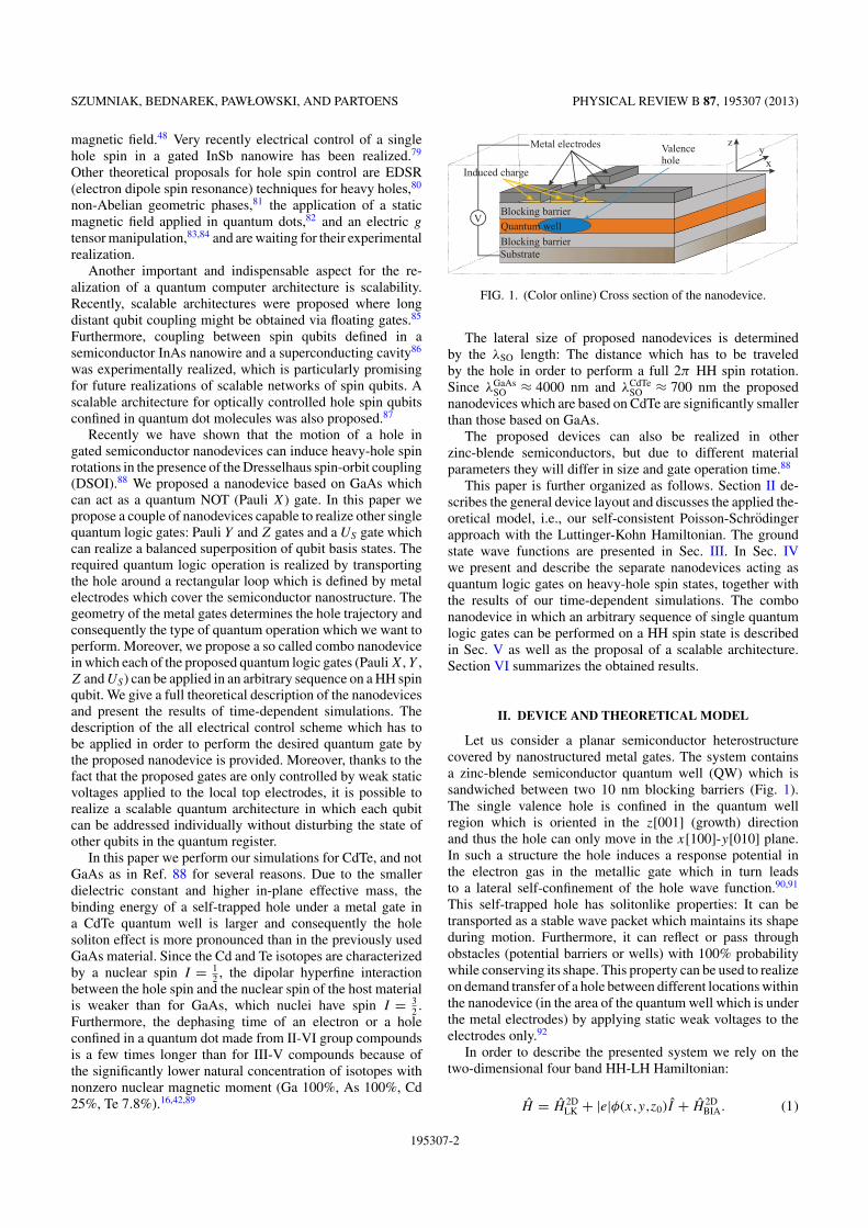
SZUMNIAK, BEDNAREK, PAWŁOWSKI, AND PARTOENS PHYSICAL REVIEW B 87, 195307 (2013)
magnetic field.48 Very recently electrical control of a singlehole spin in a gated InSb nanowire has been realized.79
Other theoretical proposals for hole spin control are EDSR(electron dipole spin resonance) techniques for heavy holes,80
non-Abelian geometric phases,81 the application of a staticmagnetic field applied in quantum dots,82 and an electric g
tensor manipulation,83,84 and are waiting for their experimentalrealization.
Another important and indispensable aspect for the re-alization of a quantum computer architecture is scalability.Recently, scalable architectures were proposed where longdistant qubit coupling might be obtained via floating gates.85
Furthermore, coupling between spin qubits defined in asemiconductor InAs nanowire and a superconducting cavity86
was experimentally realized, which is particularly promisingfor future realizations of scalable networks of spin qubits. Ascalable architecture for optically controlled hole spin qubitsconfined in quantum dot molecules was also proposed.87
Recently we have shown that the motion of a hole ingated semiconductor nanodevices can induce heavy-hole spinrotations in the presence of the Dresselhaus spin-orbit coupling(DSOI).88 We proposed a nanodevice based on GaAs whichcan act as a quantum NOT (Pauli X) gate. In this paper wepropose a couple of nanodevices capable to realize other singlequantum logic gates: Pauli Y and Z gates and a US gate whichcan realize a balanced superposition of qubit basis states. Therequired quantum logic operation is realized by transportingthe hole around a rectangular loop which is defined by metalelectrodes which cover the semiconductor nanostructure. Thegeometry of the metal gates determines the hole trajectory andconsequently the type of quantum operation which we want toperform. Moreover, we propose a so called combo nanodevicein which each of the proposed quantum logic gates (Pauli X, Y ,Z and US) can be applied in an arbitrary sequence on a HH spinqubit. We give a full theoretical description of the nanodevicesand present the results of time-dependent simulations. Thedescription of the all electrical control scheme which has tobe applied in order to perform the desired quantum gate bythe proposed nanodevice is provided. Moreover, thanks to thefact that the proposed gates are only controlled by weak staticvoltages applied to the local top electrodes, it is possible torealize a scalable quantum architecture in which each qubitcan be addressed individually without disturbing the state ofother qubits in the quantum register.
In this paper we perform our simulations for CdTe, and notGaAs as in Ref. 88 for several reasons. Due to the smallerdielectric constant and higher in-plane effective mass, thebinding energy of a self-trapped hole under a metal gate ina CdTe quantum well is larger and consequently the holesoliton effect is more pronounced than in the previously usedGaAs material. Since the Cd and Te isotopes are characterizedby a nuclear spin I = 1
2 , the dipolar hyperfine interactionbetween the hole spin and the nuclear spin of the host materialis weaker than for GaAs, which nuclei have spin I = 3
2 .Furthermore, the dephasing time of an electron or a holeconfined in a quantum dot made from II-VI group compoundsis a few times longer than for III-V compounds because ofthe significantly lower natural concentration of isotopes withnonzero nuclear magnetic moment (Ga 100%, As 100%, Cd25%, Te 7.8%).16,42,89
Valencehole x
yz
Quantum well
Blocking barrier
Blocking barrierSubstrate
Metal electrodes
V
Induced charge
FIG. 1. (Color online) Cross section of the nanodevice.
The lateral size of proposed nanodevices is determinedby the λSO length: The distance which has to be traveledby the hole in order to perform a full 2π HH spin rotation.Since λGaAs
SO ≈ 4000 nm and λCdTeSO ≈ 700 nm the proposed
nanodevices which are based on CdTe are significantly smallerthan those based on GaAs.
The proposed devices can also be realized in otherzinc-blende semiconductors, but due to different materialparameters they will differ in size and gate operation time.88
This paper is further organized as follows. Section II de-scribes the general device layout and discusses the applied the-oretical model, i.e., our self-consistent Poisson-Schrodingerapproach with the Luttinger-Kohn Hamiltonian. The groundstate wave functions are presented in Sec. III. In Sec. IVwe present and describe the separate nanodevices acting asquantum logic gates on heavy-hole spin states, together withthe results of our time-dependent simulations. The combonanodevice in which an arbitrary sequence of single quantumlogic gates can be performed on a HH spin state is describedin Sec. V as well as the proposal of a scalable architecture.Section VI summarizes the obtained results.
II. DEVICE AND THEORETICAL MODEL
Let us consider a planar semiconductor heterostructurecovered by nanostructured metal gates. The system containsa zinc-blende semiconductor quantum well (QW) which issandwiched between two 10 nm blocking barriers (Fig. 1).The single valence hole is confined in the quantum wellregion which is oriented in the z[001] (growth) directionand thus the hole can only move in the x[100]-y[010] plane.In such a structure the hole induces a response potential inthe electron gas in the metallic gate which in turn leadsto a lateral self-confinement of the hole wave function.90,91
This self-trapped hole has solitonlike properties: It can betransported as a stable wave packet which maintains its shapeduring motion. Furthermore, it can reflect or pass throughobstacles (potential barriers or wells) with 100% probabilitywhile conserving its shape. This property can be used to realizeon demand transfer of a hole between different locations withinthe nanodevice (in the area of the quantum well which is underthe metal electrodes) by applying static weak voltages to theelectrodes only.92
In order to describe the presented system we rely on thetwo-dimensional four band HH-LH Hamiltonian:
H = H 2DLK + |e|φ(x,y,z0)I + H 2D
BIA. (1)
195307-2
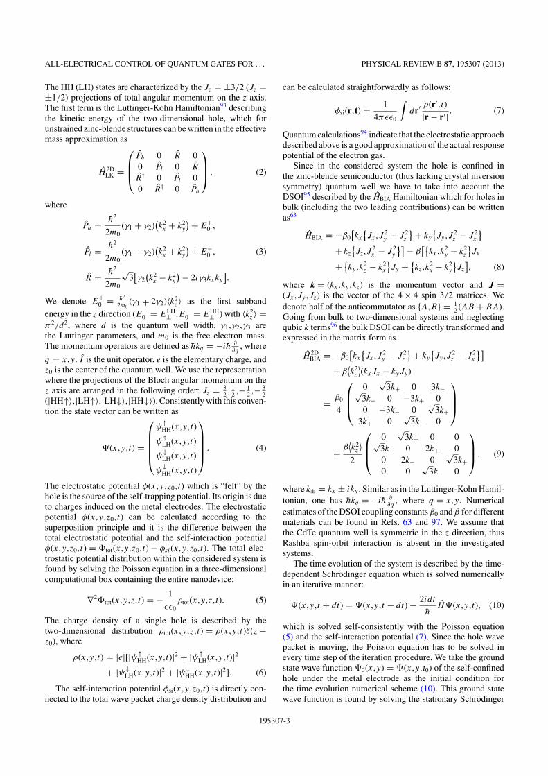
ALL-ELECTRICAL CONTROL OF QUANTUM GATES FOR . . . PHYSICAL REVIEW B 87, 195307 (2013)
The HH (LH) states are characterized by the Jz = ±3/2 (Jz =±1/2) projections of total angular momentum on the z axis.The first term is the Luttinger-Kohn Hamiltonian93 describingthe kinetic energy of the two-dimensional hole, which forunstrained zinc-blende structures can be written in the effectivemass approximation as
H 2DLK =
⎛⎜⎜⎝
Ph 0 R 00 Pl 0 R
R† 0 Pl 00 R† 0 Ph
⎞⎟⎟⎠ , (2)
where
Ph = h2
2m0(γ1 + γ2)
(k2x + k2
y
) + E+0 ,
Pl = h2
2m0(γ1 − γ2)
(k2x + k2
y
) + E−0 , (3)
R = h2
2m0
√3[γ2
(k2x − k2
y
) − 2iγ3kxky
].
We denote E±0 = h2
2m0(γ1 ∓ 2γ2)〈k2
z 〉 as the first subband
energy in the z direction (E−0 = ELH
⊥ ,E+0 = EHH
⊥ ) with 〈k2z 〉 =
π2/d2, where d is the quantum well width, γ1,γ2,γ3 arethe Luttinger parameters, and m0 is the free electron mass.The momentum operators are defined as hkq = −ih ∂
∂q, where
q = x,y. I is the unit operator, e is the elementary charge, andz0 is the center of the quantum well. We use the representationwhere the projections of the Bloch angular momentum on thez axis are arranged in the following order: Jz = 3
2 , 12 ,− 1
2 ,− 32
(|HH↑〉,|LH↑〉,|LH↓〉,|HH↓〉). Consistently with this conven-tion the state vector can be written as
�(x,y,t) =
⎛⎜⎜⎜⎜⎝
ψ↑HH(x,y,t)
ψ↑LH(x,y,t)
ψ↓LH(x,y,t)
ψ↓HH(x,y,t)
⎞⎟⎟⎟⎟⎠ . (4)
The electrostatic potential φ(x,y,z0,t) which is “felt” by thehole is the source of the self-trapping potential. Its origin is dueto charges induced on the metal electrodes. The electrostaticpotential φ(x,y,z0,t) can be calculated according to thesuperposition principle and it is the difference between thetotal electrostatic potential and the self-interaction potentialφ(x,y,z0,t) = tot(x,y,z0,t) − φsi(x,y,z0,t). The total elec-trostatic potential distribution within the considered system isfound by solving the Poisson equation in a three-dimensionalcomputational box containing the entire nanodevice:
∇2tot(x,y,z,t) = − 1
εε0ρtot(x,y,z,t). (5)
The charge density of a single hole is described by thetwo-dimensional distribution ρtot(x,y,z,t) = ρ(x,y,t)δ(z −z0), where
ρ(x,y,t) = |e|[|ψ↑HH(x,y,t)|2 + |ψ↑
LH(x,y,t)|2+ |ψ↓
LH(x,y,t)|2 + |ψ↓HH(x,y,t)|2]. (6)
The self-interaction potential φsi(x,y,z0,t) is directly con-nected to the total wave packet charge density distribution and
can be calculated straightforwardly as follows:
φsi(r,t) = 1
4πεε0
∫dr′ ρ(r′,t)
|r − r′| . (7)
Quantum calculations94 indicate that the electrostatic approachdescribed above is a good approximation of the actual responsepotential of the electron gas.
Since in the considered system the hole is confined inthe zinc-blende semiconductor (thus lacking crystal inversionsymmetry) quantum well we have to take into account theDSOI95 described by the HBIA Hamiltonian which for holes inbulk (including the two leading contributions) can be writtenas63
HBIA = −β0[kx
{Jx,J
2y − J 2
z
} + ky
{Jy,J
2z − J 2
x
}+ kz
{Jz,J
2x − J 2
y
}] − β[{
kx,k2y − k2
z
}Jx
+ {ky,k
2z − k2
x
}Jy + {
kz,k2x − k2
y
}Jz
], (8)
where k = (kx,ky,kz) is the momentum vector and J =(Jx,Jy,Jz) is the vector of the 4 × 4 spin 3/2 matrices. Wedenote half of the anticommutator as {A,B} = 1
2 (AB + BA).Going from bulk to two-dimensional systems and neglectingqubic k terms96 the bulk DSOI can be directly transformed andexpressed in the matrix form as
H 2DBIA = −β0
[kx
{Jx,J
2y − J 2
z
} + ky
{Jy,J
2z − J 2
x
}]+β
⟨k2z
⟩(kxJx − kyJy)
= β0
4
⎛⎜⎜⎝
0√
3k+ 0 3k−√3k− 0 −3k+ 00 −3k− 0
√3k+
3k+ 0√
3k− 0
⎞⎟⎟⎠
+ β⟨k2z
⟩2
⎛⎜⎜⎝
0√
3k+ 0 0√3k− 0 2k+ 00 2k− 0
√3k+
0 0√
3k− 0
⎞⎟⎟⎠ , (9)
where k± = kx ± iky . Similar as in the Luttinger-Kohn Hamil-tonian, one has hkq = −ih ∂
∂q, where q = x,y. Numerical
estimates of the DSOI coupling constants β0 and β for differentmaterials can be found in Refs. 63 and 97. We assume thatthe CdTe quantum well is symmetric in the z direction, thusRashba spin-orbit interaction is absent in the investigatedsystems.
The time evolution of the system is described by the time-dependent Schrodinger equation which is solved numericallyin an iterative manner:
�(x,y,t + dt) = �(x,y,t − dt) − 2idt
hH�(x,y,t), (10)
which is solved self-consistently with the Poisson equation(5) and the self-interaction potential (7). Since the hole wavepacket is moving, the Poisson equation has to be solved inevery time step of the iteration procedure. We take the groundstate wave function �0(x,y) = �(x,y,t0) of the self-confinedhole under the metal electrode as the initial condition forthe time evolution numerical scheme (10). This ground statewave function is found by solving the stationary Schrodinger
195307-3
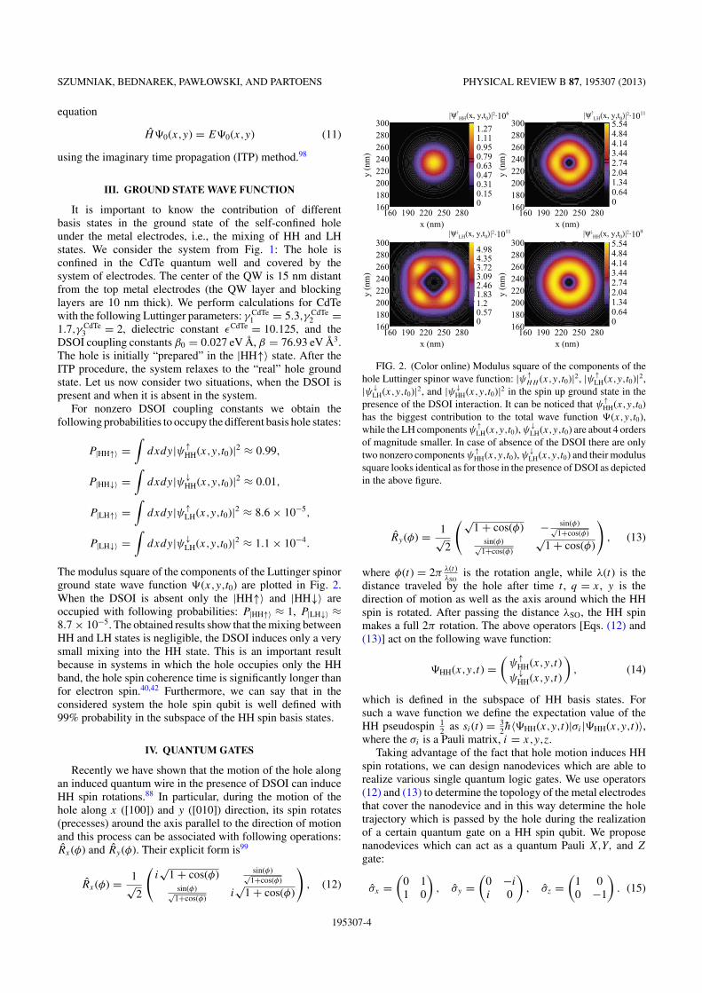
SZUMNIAK, BEDNAREK, PAWŁOWSKI, AND PARTOENS PHYSICAL REVIEW B 87, 195307 (2013)
equation
H�0(x,y) = E�0(x,y) (11)
using the imaginary time propagation (ITP) method.98
III. GROUND STATE WAVE FUNCTION
It is important to know the contribution of differentbasis states in the ground state of the self-confined holeunder the metal electrodes, i.e., the mixing of HH and LHstates. We consider the system from Fig. 1: The hole isconfined in the CdTe quantum well and covered by thesystem of electrodes. The center of the QW is 15 nm distantfrom the top metal electrodes (the QW layer and blockinglayers are 10 nm thick). We perform calculations for CdTewith the following Luttinger parameters: γ CdTe
1 = 5.3,γ CdTe2 =
1.7,γ CdTe3 = 2, dielectric constant εCdTe = 10.125, and the
DSOI coupling constants β0 = 0.027 eV A, β = 76.93 eV A3.The hole is initially “prepared” in the |HH↑〉 state. After theITP procedure, the system relaxes to the “real” hole groundstate. Let us now consider two situations, when the DSOI ispresent and when it is absent in the system.
For nonzero DSOI coupling constants we obtain thefollowing probabilities to occupy the different basis hole states:
P|HH↑〉 =∫
dxdy|ψ↑HH(x,y,t0)|2 ≈ 0.99,
P|HH↓〉 =∫
dxdy|ψ↓HH(x,y,t0)|2 ≈ 0.01,
P|LH↑〉 =∫
dxdy|ψ↑LH(x,y,t0)|2 ≈ 8.6 × 10⁻⁵,
P|LH↓〉 =∫
dxdy|ψ↓LH(x,y,t0)|2 ≈ 1.1 × 10⁻⁴.
The modulus square of the components of the Luttinger spinorground state wave function �(x,y,t0) are plotted in Fig. 2.When the DSOI is absent only the |HH↑〉 and |HH↓〉 areoccupied with following probabilities: P|HH↑〉 ≈ 1, P|LH↓〉 ≈8.7 × 10⁻⁵. The obtained results show that the mixing betweenHH and LH states is negligible, the DSOI induces only a verysmall mixing into the HH state. This is an important resultbecause in systems in which the hole occupies only the HHband, the hole spin coherence time is significantly longer thanfor electron spin.40,42 Furthermore, we can say that in theconsidered system the hole spin qubit is well defined with99% probability in the subspace of the HH spin basis states.
IV. QUANTUM GATES
Recently we have shown that the motion of the hole alongan induced quantum wire in the presence of DSOI can induceHH spin rotations.88 In particular, during the motion of thehole along x ([100]) and y ([010]) direction, its spin rotates(precesses) around the axis parallel to the direction of motionand this process can be associated with following operations:Rx(φ) and Ry(φ). Their explicit form is99
Rx(φ) = 1√2
(i√
1 + cos(φ) sin(φ)√1+cos(φ)
sin(φ)√1+cos(φ)
i√
1 + cos(φ)
), (12)
160 190 220 250 280x (nm)
160180200220240260280300
y (n
m)
00.641.342.042.743.444.144.845.54
160 190 220 250 280x (nm)
160180200220240260280300
y (n
m)
00.571.21.832.463.093.724.354.98
160 190 220 250 280x (nm)
160180200220240260280300
y (n
m)
00.641.342.042.743.444.144.845.54
160 190 220 250 280x (nm)
160180200220240260280300
y (n
m)
00.150.310.470.630.790.951.111.27
|ψ HH(x, y,t0)|2.106 |ψ LH(x, y,t0)|2.1011
|ψ LH(x, y,t0)|2.1011 |ψ HH(x, y,t0)|2.109
FIG. 2. (Color online) Modulus square of the components of thehole Luttinger spinor wave function: |ψ↑
HH (x,y,t0)|2, |ψ↑LH(x,y,t0)|2,
|ψ↓LH(x,y,t0)|2, and |ψ↓
HH(x,y,t0)|2 in the spin up ground state in thepresence of the DSOI interaction. It can be noticed that ψ
↑HH(x,y,t0)
has the biggest contribution to the total wave function �(x,y,t0),while the LH components ψ
↑LH(x,y,t0), ψ↓
LH(x,y,t0) are about 4 ordersof magnitude smaller. In case of absence of the DSOI there are onlytwo nonzero components ψ
↑HH(x,y,t0), ψ↓
LH(x,y,t0) and their modulussquare looks identical as for those in the presence of DSOI as depictedin the above figure.
Ry(φ) = 1√2
(√1 + cos(φ) − sin(φ)√
1+cos(φ)sin(φ)√
1+cos(φ)
√1 + cos(φ)
), (13)
where φ(t) = 2π λ(t)λSO
is the rotation angle, while λ(t) is thedistance traveled by the hole after time t , q = x, y is thedirection of motion as well as the axis around which the HHspin is rotated. After passing the distance λSO, the HH spinmakes a full 2π rotation. The above operators [Eqs. (12) and(13)] act on the following wave function:
�HH(x,y,t) =(
ψ↑HH(x,y,t)
ψ↓HH(x,y,t)
), (14)
which is defined in the subspace of HH basis states. Forsuch a wave function we define the expectation value of theHH pseudospin 1
2 as si(t) = 32h〈�HH(x,y,t)|σi |�HH(x,y,t)〉,
where the σi is a Pauli matrix, i = x,y,z.Taking advantage of the fact that hole motion induces HH
spin rotations, we can design nanodevices which are able torealize various single quantum logic gates. We use operators(12) and (13) to determine the topology of the metal electrodesthat cover the nanodevice and in this way determine the holetrajectory which is passed by the hole during the realizationof a certain quantum gate on a HH spin qubit. We proposenanodevices which can act as a quantum Pauli X,Y, and Z
gate:
σx =(
0 11 0
), σy =
(0 −i
i 0
), σz =
(1 00 −1
). (15)
195307-4
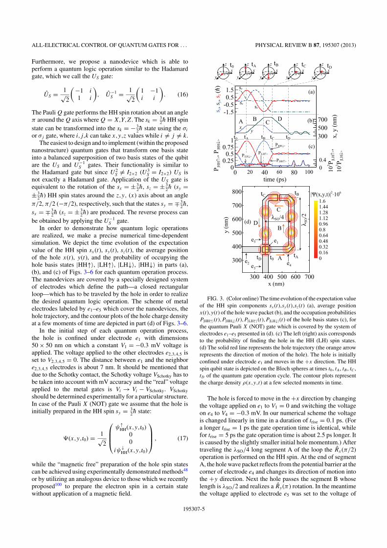
ALL-ELECTRICAL CONTROL OF QUANTUM GATES FOR . . . PHYSICAL REVIEW B 87, 195307 (2013)
Furthermore, we propose a nanodevice which is able toperform a quantum logic operation similar to the Hadamardgate, which we call the US gate:
US = 1√2
(−1 i
1 i
), U−1
S = 1√2
(1 −1i i
). (16)
The Pauli Q gate performs the HH spin rotation about an angleπ around the Q axis where Q = X,Y,Z. The sk = 3
2h HH spinstate can be transformed into the sk = − 3
2h state using the σi
or σj gate, where i,j,k can take x,y,z values while i �= j �= k.The easiest to design and to implement (within the proposed
nanostructure) quantum gates that transform one basis stateinto a balanced superposition of two basis states of the qubitare the US and U−1
S gates. Their functionality is similar tothe Hadamard gate but since U 2
S �= I2×2 (U 3S = I2×2) US is
not exactly a Hadamard gate. Application of the US gate isequivalent to the rotation of the sx = ± 3
2h, sz = ± 32h (sy =
± 32h) HH spin states around the z,y, (x) axis about an angle
π/2, π/2 (−π/2), respectively, such that the states sy = ∓ 32h,
sx = ∓ 32h (sz = ± 3
2h) are produced. The reverse process canbe obtained by applying the U−1
S gate.In order to demonstrate how quantum logic operations
are realized, we make a precise numerical time-dependentsimulation. We depict the time evolution of the expectationvalue of the HH spin sx(t), sy(t), sz(t), the average positionof the hole x(t), y(t), and the probability of occupying thehole basis states |HH↑〉, |LH↑〉, |LH↓〉, |HH↓〉 in parts (a),(b), and (c) of Figs. 3–6 for each quantum operation process.The nanodevices are covered by a specially designed systemof electrodes which define the path—a closed rectangularloop—which has to be traveled by the hole in order to realizethe desired quantum logic operation. The scheme of metalelectrodes labeled by e1–e5 which cover the nanodevices, thehole trajectory, and the contour plots of the hole charge densityat a few moments of time are depicted in part (d) of Figs. 3–6.
In the initial step of each quantum operation process,the hole is confined under electrode e1 with dimensions50 × 50 nm on which a constant V1 = −0.3 mV voltage isapplied. The voltage applied to the other electrodes e2,3,4,5 isset to V2,3,4,5 = 0. The distance between e1 and the neighbore2,3,4,5 electrodes is about 7 nm. It should be mentioned thatdue to the Schotky contact, the Schotky voltage VSchotky has tobe taken into account with mV accuracy and the “real” voltageapplied to the metal gates is Vi → Vi − VSchotky. VSchotky
should be determined experimentally for a particular structure.In case of the Pauli X (NOT) gate we assume that the hole isinitially prepared in the HH spin sy = 3
2h state:
�(x,y,t0) = 1√2
⎛⎜⎜⎝
ψ↑HH(x,y,t0)
00
iψ↓HH(x,y,t0)
⎞⎟⎟⎠ , (17)
while the “magnetic free” preparation of the hole spin statescan be achieved using experimentally demonstrated methods48
or by utilizing an analogous device to those which we recentlyproposed100 to prepare the electron spin in a certain statewithout application of a magnetic field.
300 400 500 600 700
300
400
500
600
700
800
00.160.320.480.640.80.961.121.281.441.6
e1
e2e3
e4
A
B
C
D λ SO/2λSO/4
t0tA
tBtC
tD
e5
x (nm)
y (n
m)
(d)
0 40 8020 60 100time (ps)
00.250.5
0.751
P|H
H↑>
, P|H
H↓>
103 P
|LH
↑>,
103 P
|LH
↓>
300500700
x, y
(nm
)-1.5-0.50.51.5
s x, s
y, s z
(h)
P|HH↑>
P|HH↓>
sy
sz
sx
xy
P|LH↑>P|LH↓>
A BC
D
(a)
(b)
(c)
0
0.4
t0 tB tC tDtA
t0 z
x
y
tA zx
y
tB zx
y
tC zx
y
tD z
x
y
|Ψ(x,y,t)|2.106
FIG. 3. (Color online) The time evolution of the expectation valueof the HH spin components sx(t),sy(t),sz(t) (a), average positionx(t),y(t) of the hole wave packet (b), and the occupation probabilitiesP|HH↑〉(t),P|HH↓〉(t),P|LH↑〉(t),P|LH↓〉(t) of the hole basis states (c), forthe quantum Pauli X (NOT) gate which is covered by the system ofelectrodes e1–e5 presented in (d). (c) The left (right) axis correspondsto the probability of finding the hole in the HH (LH) spin states.(d) The solid red line represents the hole trajectory (the orange arrowrepresents the direction of motion of the hole). The hole is initiallyconfined under electrode e1 and moves in the +x direction. The HHspin qubit state is depicted on the Bloch spheres at times t0, tA, tB , tC ,tD of the quantum gate operation cycle. The contour plots representthe charge density ρ(x,y,t) at a few selected moments in time.
The hole is forced to move in the +x direction by changingthe voltage applied on e1 to V1 = 0 and switching the voltageon e4 to V4 = −0.3 mV. In our numerical scheme the voltageis changed linearly in time in a duration of trise = 0.1 ps. (Fora longer trise = 1 ps the gate operation time is identical, whilefor trise = 5 ps the gate operation time is about 2.5 ps longer. Itis caused by the slightly smaller initial hole momentum.) Aftertraveling the λSO/4 long segment A of the loop the Rx(π/2)operation is performed on the HH spin. At the end of segmentA, the hole wave packet reflects from the potential barrier at thecorner of electrode e4 and changes its direction of motion intothe +y direction. Next the hole passes the segment B whoselength is λSO/2 and realizes a Ry(π ) rotation. In the meantimethe voltage applied to electrode e5 was set to the voltage of
195307-5
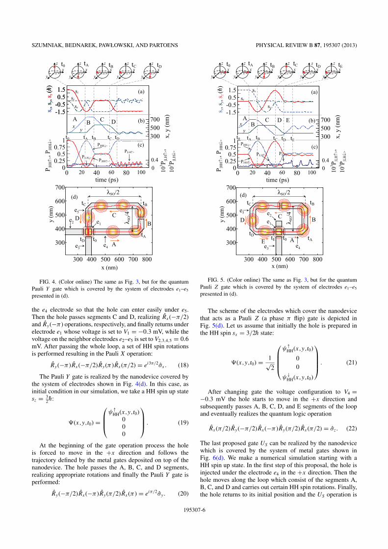
SZUMNIAK, BEDNAREK, PAWŁOWSKI, AND PARTOENS PHYSICAL REVIEW B 87, 195307 (2013)
300 400 500 600 700 800
300
400
500
600
700
e1
e3
e2
e4
D C
B
A
λSO/2
λ SO/4
tD
tC tB
tAt0
103 P
|LH
↑>,
103 P
|LH
↓>
300500700
x, y
(nm
)-1.5-0.50.51.5
s x, s
y, s z
(h)
-1.5-0.50.51.5
s x, s
y, s z
(h)
0 40 8020 60 100time (ps)
00.25
0.50.75
1
P|H
H↑>
, P|H
H↓>
P|HH↑>
P|HH↓>
sy
sz
sx
xy
P|LH↑>
P|LH↓>
AB C D
(a)
(b)
(c)
0
0.4
t0 tB tC tDtA
e5
x (nm)
y (n
m)
(d)
t0 z
x
y
tA zx
y
tB z
x
y
tC z
x
y
tD z
x
y
FIG. 4. (Color online) The same as Fig. 3, but for the quantumPauli Y gate which is covered by the system of electrodes e1–e5
presented in (d).
the e4 electrode so that the hole can enter easily under e5.Then the hole passes segments C and D, realizing Rx(−π/2)and Ry(−π ) operations, respectively, and finally returns underelectrode e1 whose voltage is set to V1 = −0.3 mV, while thevoltage on the neighbor electrodes e2–e5 is set to V2,3,4,5 = 0.6mV. After passing the whole loop, a set of HH spin rotationsis performed resulting in the Pauli X operation:
Ry(−π )Rx(−π/2)Ry(π )Rx(π/2) = ei3π/2σx . (18)
The Pauli Y gate is realized by the nanodevice covered bythe system of electrodes shown in Fig. 4(d). In this case, asinitial condition in our simulation, we take a HH spin up statesz = 3
2h:
�(x,y,t0) =
⎛⎜⎜⎝
ψ↑HH(x,y,t0)
000
⎞⎟⎟⎠ . (19)
At the beginning of the gate operation process the holeis forced to move in the +x direction and follows thetrajectory defined by the metal gates deposited on top of thenanodevice. The hole passes the A, B, C, and D segments,realizing appropriate rotations and finally the Pauli Y gate isperformed:
Ry(−π/2)Rx(−π )Ry(π/2)Rx(π ) = eiπ/2σy . (20)
300 400 500 600 700 800
300
400
500
600
700
e1
e3
e2
e4
A
BCD
λSO/2
λ SO/4
t0 tA
tBtC
tD
103 P
|LH
↑>,
103 P
|LH
↓ >
300500700
x, y
(nm
)-1.5-0.50.51.5
s x, s
y, s z
(h)
0 40 8020 60 100time (ps)
00.25
0.50.75
1
P|H
H↑>
, P|H
H↓>
P|HH↑>
P|HH↓>
sy
sz
sx
xy
P|LH↑> P|LH↓>
AB
C D
(a)
(b)
(c)
0
0.4
t0 tB tC tEtA
e5
x (nm)
y (n
m)
(d)
tEE
E
t0 z
x
y
tA zx
y
tB z
x
y
tC zx
y
tEx
y
z z tDx
y
tD
FIG. 5. (Color online) The same as Fig. 3, but for the quantumPauli Z gate which is covered by the system of electrodes e1–e5
presented in (d).
The scheme of the electrodes which cover the nanodevicethat acts as a Pauli Z (a phase π flip) gate is depicted inFig. 5(d). Let us assume that initially the hole is prepared inthe HH spin sx = 3/2h state:
�(x,y,t0) = 1√2
⎛⎜⎜⎜⎝
ψ↑HH(x,y,t0)
00
ψ↓HH(x,y,t0)
⎞⎟⎟⎟⎠ . (21)
After changing gate the voltage configuration to V4 =−0.3 mV the hole starts to move in the +x direction andsubsequently passes A, B, C, D, and E segments of the loopand eventually realizes the quantum logic operation
Rx(π/2)Ry(−π/2)Rx(−π )Ry(π/2)Rx(π/2) = σz. (22)
The last proposed gate US can be realized by the nanodevicewhich is covered by the system of metal gates shown inFig. 6(d). We make a numerical simulation starting with aHH spin up state. In the first step of this proposal, the hole isinjected under the electrode e4 in the +x direction. Then thehole moves along the loop which consist of the segments A,B, C, and D and carries out certain HH spin rotations. Finally,the hole returns to its initial position and the US operation is
195307-6
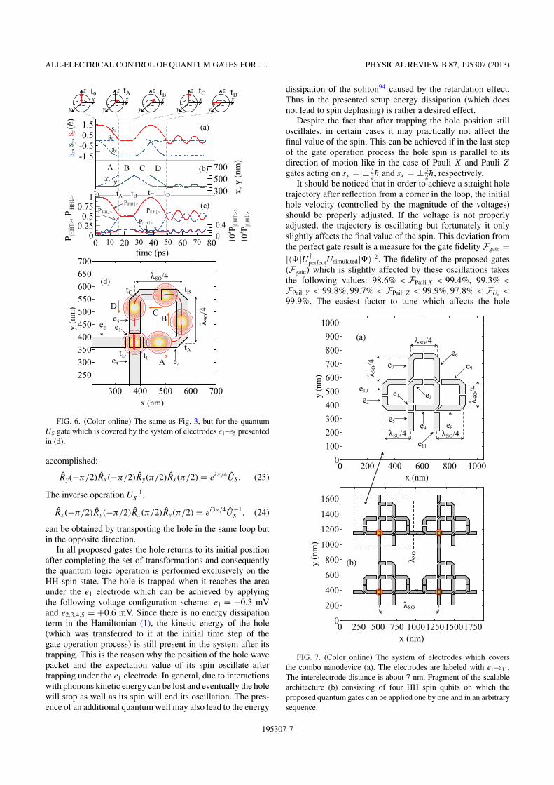
ALL-ELECTRICAL CONTROL OF QUANTUM GATES FOR . . . PHYSICAL REVIEW B 87, 195307 (2013)
300 400 500 600 700
250
300
350
400
450
500
550
600
650
700
103 P
|LH
↑>,
103 P
|LH
↓ >
300500700
x, y
(nm
)-1.5-0.50.51.5
s x, s
y, s z
(h)
0 20 40 60 8010 30 50 70time (ps)
00.250.5
0.751
P|H
H↑>
, P|H
H↓> P|HH↑>
P|HH↓>
sy
sz
sx
x y
P|LH↑>
P|LH↓>
A B C D
(a)
(b)
(c)
0
0.4
t0 tB tC tDtA
t0 z
x
y
tA zx
y
tB z
x
y
tC zx
y
tD z
x
y
e1
e3
e2
e4A
BC
D
λSO/4
λ SO/4
t0
tA
tBtC
tD
e5
x (nm)
y (n
m)
(d)
FIG. 6. (Color online) The same as Fig. 3, but for the quantumUS gate which is covered by the system of electrodes e1–e5 presentedin (d).
accomplished:
Ry(−π/2)Rx(−π/2)Ry(π/2)Rx(π/2) = eiπ/4US. (23)
The inverse operation U−1S ,
Rx(−π/2)Ry(−π/2)Rx(π/2)Ry(π/2) = ei3π/4U−1S , (24)
can be obtained by transporting the hole in the same loop butin the opposite direction.
In all proposed gates the hole returns to its initial positionafter completing the set of transformations and consequentlythe quantum logic operation is performed exclusively on theHH spin state. The hole is trapped when it reaches the areaunder the e1 electrode which can be achieved by applyingthe following voltage configuration scheme: e1 = −0.3 mVand e2,3,4,5 = +0.6 mV. Since there is no energy dissipationterm in the Hamiltonian (1), the kinetic energy of the hole(which was transferred to it at the initial time step of thegate operation process) is still present in the system after itstrapping. This is the reason why the position of the hole wavepacket and the expectation value of its spin oscillate aftertrapping under the e1 electrode. In general, due to interactionswith phonons kinetic energy can be lost and eventually the holewill stop as well as its spin will end its oscillation. The pres-ence of an additional quantum well may also lead to the energy
dissipation of the soliton94 caused by the retardation effect.Thus in the presented setup energy dissipation (which doesnot lead to spin dephasing) is rather a desired effect.
Despite the fact that after trapping the hole position stilloscillates, in certain cases it may practically not affect thefinal value of the spin. This can be achieved if in the last stepof the gate operation process the hole spin is parallel to itsdirection of motion like in the case of Pauli X and Pauli Z
gates acting on sy = ± 32h and sx = ± 3
2h, respectively.It should be noticed that in order to achieve a straight hole
trajectory after reflection from a corner in the loop, the initialhole velocity (controlled by the magnitude of the voltages)should be properly adjusted. If the voltage is not properlyadjusted, the trajectory is oscillating but fortunately it onlyslightly affects the final value of the spin. This deviation fromthe perfect gate result is a measure for the gate fidelity Fgate =|〈�|U †
perfectUsimulated|�〉|2. The fidelity of the proposed gates(Fgate) which is slightly affected by these oscillations takesthe following values: 98.6% < FPaili X < 99.4%, 99.3% <
FPaili Y < 99.8%, 99.7% < FPaili Z < 99.9%, 97.8% < FUs<
99.9%. The easiest factor to tune which affects the hole
0 200 400 600 800 10000
100
200
300
400
500
600
700
800
900
1000
x (nm)
y (n
m)
e1
e4
e3
e5
e6
e2
e7
e8
e9
e10
e11
λSO/4 λSO/4
λSO/4
λ SO/4
λ SO/4
(a)
(b)
0 250 500 750 1000125015001750x (nm)
0
200
400
600
800
1000
1200
1400
1600
y (n
m)
λ SO
λSO
FIG. 7. (Color online) The system of electrodes which coversthe combo nanodevice (a). The electrodes are labeled with e1–e11.The interelectrode distance is about 7 nm. Fragment of the scalablearchitecture (b) consisting of four HH spin qubits on which theproposed quantum gates can be applied one by one and in an arbitrarysequence.
195307-7
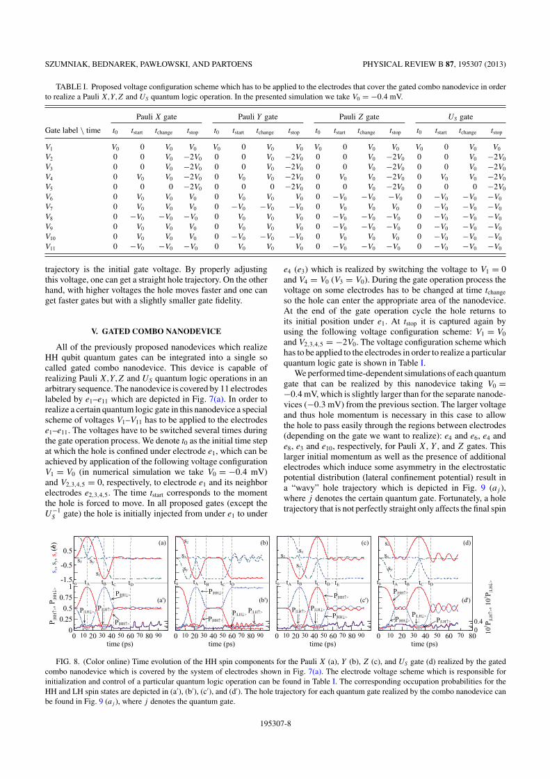
SZUMNIAK, BEDNAREK, PAWŁOWSKI, AND PARTOENS PHYSICAL REVIEW B 87, 195307 (2013)
TABLE I. Proposed voltage configuration scheme which has to be applied to the electrodes that cover the gated combo nanodevice in orderto realize a Pauli X,Y,Z and US quantum logic operation. In the presented simulation we take V0 = −0.4 mV.
Pauli X gate Pauli Y gate Pauli Z gate US gate
Gate label \ time t0 tstart tchange tstop t0 tstart tchange tstop t0 tstart tchange tstop t0 tstart tchange tstop
V1 V0 0 V0 V0 V0 0 V0 V0 V0 0 V0 V0 V0 0 V0 V0
V2 0 0 V0 −2V0 0 0 V0 −2V0 0 0 V0 −2V0 0 0 V0 −2V0
V3 0 0 V0 −2V0 0 0 V0 −2V0 0 0 V0 −2V0 0 0 V0 −2V0
V4 0 V0 V0 −2V0 0 V0 V0 −2V0 0 V0 V0 −2V0 0 V0 V0 −2V0
V5 0 0 0 −2V0 0 0 0 −2V0 0 0 V0 −2V0 0 0 0 −2V0
V6 0 V0 V0 V0 0 V0 V0 V0 0 −V0 −V0 −V0 0 −V0 −V0 −V0
V7 0 V0 V0 V0 0 −V0 −V0 −V0 0 V0 V0 V0 0 −V0 −V0 −V0
V8 0 −V0 −V0 −V0 0 V0 V0 V0 0 −V0 −V0 −V0 0 −V0 −V0 −V0
V9 0 V0 V0 V0 0 V0 V0 V0 0 −V0 −V0 −V0 0 −V0 −V0 −V0
V10 0 V0 V0 V0 0 −V0 −V0 −V0 0 V0 V0 V0 0 −V0 −V0 −V0
V11 0 −V0 −V0 −V0 0 V0 V0 V0 0 −V0 −V0 −V0 0 −V0 −V0 −V0
trajectory is the initial gate voltage. By properly adjustingthis voltage, one can get a straight hole trajectory. On the otherhand, with higher voltages the hole moves faster and one canget faster gates but with a slightly smaller gate fidelity.
V. GATED COMBO NANODEVICE
All of the previously proposed nanodevices which realizeHH qubit quantum gates can be integrated into a single socalled gated combo nanodevice. This device is capable ofrealizing Pauli X,Y,Z and US quantum logic operations in anarbitrary sequence. The nanodevice is covered by 11 electrodeslabeled by e1–e11 which are depicted in Fig. 7(a). In order torealize a certain quantum logic gate in this nanodevice a specialscheme of voltages V1–V11 has to be applied to the electrodese1–e11. The voltages have to be switched several times duringthe gate operation process. We denote t0 as the initial time stepat which the hole is confined under electrode e1, which can beachieved by application of the following voltage configurationV1 = V0 (in numerical simulation we take V0 = −0.4 mV)and V2,3,4,5 = 0, respectively, to electrode e1 and its neighborelectrodes e2,3,4,5. The time tstart corresponds to the momentthe hole is forced to move. In all proposed gates (except theU−1
S gate) the hole is initially injected from under e1 to under
e4 (e3) which is realized by switching the voltage to V1 = 0and V4 = V0 (V3 = V0). During the gate operation process thevoltage on some electrodes has to be changed at time tchange
so the hole can enter the appropriate area of the nanodevice.At the end of the gate operation cycle the hole returns toits initial position under e1. At tstop it is captured again byusing the following voltage configuration scheme: V1 = V0
and V2,3,4,5 = −2V0. The voltage configuration scheme whichhas to be applied to the electrodes in order to realize a particularquantum logic gate is shown in Table I.
We performed time-dependent simulations of each quantumgate that can be realized by this nanodevice taking V0 =−0.4 mV, which is slightly larger than for the separate nanode-vices (−0.3 mV) from the previous section. The larger voltageand thus hole momentum is necessary in this case to allowthe hole to pass easily through the regions between electrodes(depending on the gate we want to realize): e4 and e6, e4 ande8, e3 and e10, respectively, for Pauli X, Y , and Z gates. Thislarger initial momentum as well as the presence of additionalelectrodes which induce some asymmetry in the electrostaticpotential distribution (lateral confinement potential) result ina “wavy” hole trajectory which is depicted in Fig. 9 (aj ),where j denotes the certain quantum gate. Fortunately, a holetrajectory that is not perfectly straight only affects the final spin
103 P
|LH
↑>, 1
03 P|L
H↓>
103 P
|LH
↓>
0 20 40 60 8010 30 50 70time (ps)
sy
sz
sx
(d)
(d')
t0 tB tC tDtA
0 20 40 60 8010 30 50 70 90time (ps)
sy
szsx
(c)
(c')
t0 tB tCtA
0 20 40 60 8010 30 50 70 90time (ps)
sy
sz
sx
(b)
(b')
t0 tB tC tDtA
00.4
0 20 40 60 8010 30 50 70 90time (ps)
0
0.25
0.5
0.75
1
P|H
H↑>
, P|H
H↓ >
-1.5
-0.5
0.5
s x, s
y, s z
( h)
P|HH↑>
P|HH↓>
sy
sz
sx
P|LH↑>P|LH↓>
(a)
(a')
t0 tB tC tDtA tD tE
P|HH↑>
P|HH↓>
P|LH↑>P|LH↓>
P|HH↑>
P|HH↓>
P|LH↑>P|LH↓>
P|HH↑>
P|HH↓> P|LH↑>
P|LH↓>
FIG. 8. (Color online) Time evolution of the HH spin components for the Pauli X (a), Y (b), Z (c), and US gate (d) realized by the gatedcombo nanodevice which is covered by the system of electrodes shown in Fig. 7(a). The electrode voltage scheme which is responsible forinitialization and control of a particular quantum logic operation can be found in Table I. The corresponding occupation probabilities for theHH and LH spin states are depicted in (a′), (b′), (c′), and (d′). The hole trajectory for each quantum gate realized by the combo nanodevice canbe found in Fig. 9 (aj ), where j denotes the quantum gate.
195307-8
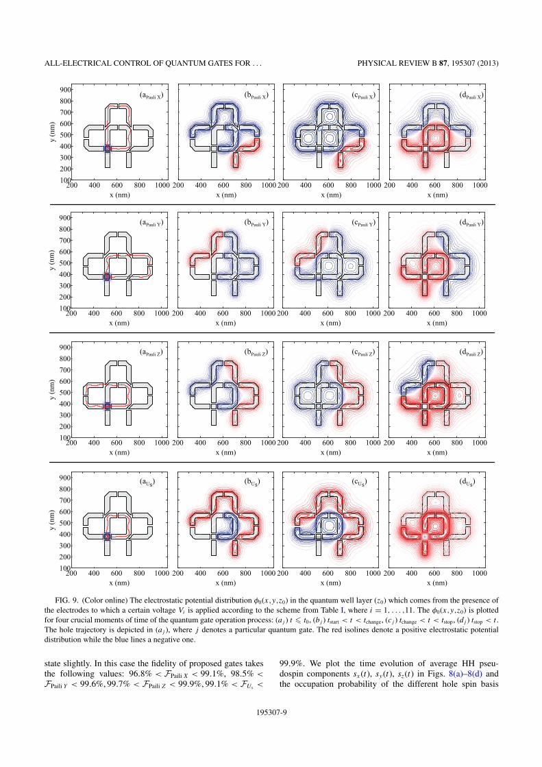
ALL-ELECTRICAL CONTROL OF QUANTUM GATES FOR . . . PHYSICAL REVIEW B 87, 195307 (2013)
200 400 600 800 1000x (nm)
100
200
300
400
500
600
700
800
900
y (n
m)
200 400 600 800 1000x (nm)
200 400 600 800 1000x (nm)
200 400 600 800 1000x (nm)
200 400 600 800 1000x (nm)
100
200
300
400
500
600
700
800
900
y (n
m)
200 400 600 800 1000x (nm)
200 400 600 800 1000x (nm)
200 400 600 800 1000x (nm)
200 400 600 800 1000x (nm)
100
200
300
400
500
600
700
800
900
y (n
m)
200 400 600 800 1000x (nm)
200 400 600 800 1000x (nm)
200 400 600 800 1000x (nm)
200 400 600 800 1000x (nm)
100
200
300
400
500
600
700
800
900
y (n
m)
200 400 600 800 1000x (nm)
200 400 600 800 1000x (nm)
200 400 600 800 1000x (nm)
(aPauli X b() Pauli X c() Pauli X d() Pauli X)
(aPauli Y b() Pauli Y c() Pauli Y d() Pauli Y)
(aPauli Z b() Pauli Z c() Pauli Z d() Pauli Z)
(aUs b() Us c() Us d() Us)
FIG. 9. (Color online) The electrostatic potential distribution φ0(x,y,z0) in the quantum well layer (z0) which comes from the presence ofthe electrodes to which a certain voltage Vi is applied according to the scheme from Table I, where i = 1, . . . ,11. The φ0(x,y,z0) is plottedfor four crucial moments of time of the quantum gate operation process: (aj ) t � t0, (bj ) tstart < t < tchange, (cj ) tchange < t < tstop, (dj ) tstop < t .The hole trajectory is depicted in (aj ), where j denotes a particular quantum gate. The red isolines denote a positive electrostatic potentialdistribution while the blue lines a negative one.
state slightly. In this case the fidelity of proposed gates takesthe following values: 96.8% < FPaili X < 99.1%, 98.5% <
FPaili Y < 99.6%, 99.7% < FPaili Z < 99.9%, 99.1% < FUs<
99.9%. We plot the time evolution of average HH pseu-dospin components sx(t), sy(t), sz(t) in Figs. 8(a)–8(d) andthe occupation probability of the different hole spin basis
195307-9
SZUMNIAK, BEDNAREK, PAWŁOWSKI, AND PARTOENS PHYSICAL REVIEW B 87, 195307 (2013)
states: P|HH↑〉(t),P|HH↓〉(t),P|LH↑〉(t),P|LH↓〉(t) can be foundin Figs. 8(a′)–8(d′) for each quantum gate cycle (Pauli X,Y , Z and US) realized by the proposed combo nanodevice.Application of the gate voltages as well as its geometry definethe path which is passed by the hole. The area under a positivelycharged electrode forms a barrier for the moving hole whilea negatively charged electrode forms a potential well withinwhich the hole can be transported. In order to illustrate howthe gate voltage influences the hole trajectory, we plot theelectrostatic potential distribution φ0(x,y,z0) in the quantumwell region which comes from the presence of the electrodesand gate voltages applied to them at four crucial momentst < t0, tstart < t < tchange, tchange < t < tstop <, tstop < t foreach (Pauli X, Y , Z and US) gate cycle. The electrostaticpotential φ0(x,y,z0) is the solution of Laplace equation in thequantum well (z0) region
∇2φ0(x,y,z) = 0, (25)
with boundary conditions determined by the presence ofthe electrodes φ0(x,y,zelectrodes) = V1–11. We have plottedφ0(x,y,z0) in Fig. 9.
In the presence of the hole there is an additional dip inthe electrostatic distribution localized in the center of the holewave packet and as the hole moves this dip follows the hole(self-trapping mechanism). The total potential which is felt bythe hole in the quantum well region was defined in Sec. II as(x,y,z0,t).
For the presented electric control scheme tchange correspondsto a different moment of time for each quantum logic gate. Incase of the Pauli X gate it is reasonable to change the voltagewhen the hole is in the area between the e6 and e7 electrode andit is done in the numerical simulation at tchange ≈ 35 ps. For thePauli Y gate process it is convenient to choose tchange ≈ 35 ps,when the hole is between the electrodes e8 and e9. Whenthe nanodevice realizes the Pauli Z or US (U−1
S ) gate, thevoltage is changed at tchange ≈ 15 ps when the hole is underelectrode e4 (it is in the middle of e3 at tchange ≈ 10 ps) justafter the reflection from the first corner. The hole is stopped attstop ≈ 60 ps, tstop ≈ 60 ps, tstop ≈ 63 ps, and tstop ≈ 44 ps forPauli X, Y , Z and US gates, respectively.
The fact that in the proposed device the quantum operationsare controlled only by the weak constant voltages appliedto locally defined electrodes allows for the realization of ascalable architecture. In Fig. 7(b) we plot the systems ofelectrodes for a scalable system of HH qubits on which eachof the proposed gates can be applied in an individual, selectivemanner.
Furthermore, the proposed device is suitable for coherenttransport of a hole wave packet and thus allows for transferringquantum information between different locations within thenanodevice. Thanks to this property two qubit gates can be
realized by transporting a hole from one induced quantum dotto another one so that the two holes can occupy the same region(the hole wave functions can overlap), for example under elec-trode e1, for a certain time t . Thanks to the exchange interactiontheir spins can swap according to the Heisenberg exchangeHamiltonian Hs(t) = J (t) �S1 · �S2 similar as two electron qubitgates are realized in two electron double quantum dots. Moredetails about two electron and hole soliton dynamics as well astwo qubit gate implementation in induced quantum dots andwires will be published in a forthcoming paper.
VI. SUMMARY
In conclusion, we proposed a set of nanodevices which canact as single quantum logic gates (Pauli X, Y , Z and US)and a combo nanodevice which is capable to perform anyof the Pauli X, Y , Z and US gate operations in an arbitrarysequence on a HH spin qubit. Quantum logic operations canbe realized all electrically and ultrafast, i.e., within 70 ps. Theproposed devices are based on induced quantum dots and wireswhich allow for transporting the hole in the form of a stablesolitonlike wave packet, while the hole trajectory is determinedby the geometry and voltages applied to the top electrodes.The motion of the hole along specially designed paths in thepresence of the Dresselhaus spin-orbit field is equivalent tothe sequential application of static magnetic fields which rotatethe HH spin qubit. This control method allows us to avoid theapplication of real magnetic fields which, because of the verysmall hole in-plane g factor, have to be of the order of severalTeslas, which is still experimentally challenging to achieve.
Since quantum gates are controlled only by low staticelectric fields generated by the local top electrodes, ourproposal can be extended to a larger number of qubits storedin the quantum register as in Fig. 7(b) where each qubit canbe manipulated individually. Therefore, a scalable architecturecan be realized. Furthermore, the proposed device is suitablefor coherent transport of a hole wave packet, and thus allows fortransferring quantum information between different locationsin the nanodevice which gives perspective to couple longdistant HH spin qubits and realize two qubit quantum gatesin this proposed scalable system.
ACKNOWLEDGMENTS
This work was supported by the Polish National ScienceCenter (Grant No. DEC-2011/03/N/ST3/02963), as well asby the “Krakow Interdisciplinary PhD-Project in Nanoscienceand Advanced Nanostructures” operated within the Founda-tion for Polish Science MPD Programme, co-financed by theEuropean Regional Development Fund. This research wassupported in part by PL-Grid Infrastructure.
*[email protected]. Awshalom, D. Loss, and N. Samarth, Semiconductor Spintron-ics and Quantum Computation (Springer, Berlin, 2002).
2I. Zutic, J. Fabian, and S. Das Sarma, Rev. Mod. Phys. 76, 323(2004).
3D. Loss and D. P. DiVincenzo, Phys. Rev. A 57, 120(1998).
4R. Hanson, L. P. Kouwenhoven, J. R. Petta, S. Tarucha,and L. M. K. Vandersypen, Rev. Mod. Phys. 79, 1217(2007).
195307-10
ALL-ELECTRICAL CONTROL OF QUANTUM GATES FOR . . . PHYSICAL REVIEW B 87, 195307 (2013)
5S. Amasha, K. MacLean, I. P. Radu, D. M. Zumbuhl, M. A. Kastner,M. P. Hanson, and A. C. Gossard, Phys. Rev. Lett. 100, 046803(2008).
6J. R. Petta, A. C. Johnson, J. M. Taylor, E. A. Laird, A. Yacoby,M. D. Lukin, C. M. Marcus, M. P. Hanson, and A. C. Gossard,Science 309, 2180 (2005).
7J. M. Elzerman, R. Hanson, L. H. Willems van Beveren,B. Witkamp, L. M. K. Vandersypen, and L. P. Kouwenhoven,Nature (London) 430, 431 (2004).
8T. Meunier, I. T. Vink, L. H. W. van Beveren, F. H. L. Koppens,H. P. Tranitz, W. Wegscheider, L. P. Kouwenhoven, and L. M. K.Vandersypen, Phys. Rev. B 74, 195303 (2006).
9F. H. L. Koppens, C. Buizert, K. J. Tielrooij, I. T. Vink,K. C. Nowack, T. Meunier, L. P. Kouwenhoven, and L. M. K.Vandersypen, Nature (London) 442, 766 (2006).
10A. Morello, J. J. Pla, F. A. Zwanenburg, K. W. Chan, K. Y. Tan,H. Huebl, M. Mottonen, C. D. Nugroho, C. Yang, J. A. vanDonkelaar, A. D. C. Alves, D. N. Jamieson, C. C. Escott, L. C.L. Hollenberg, R. G. Clark, and A. S. Dzurak, Nature (London)467, 687 (2010).
11K. C. Nowack, F. H. L. Koppens, Yu. V. Nazarov, and L. M. K.Vandersypen, Science 318, 1430 (2007).
12S. Nadj-Perge, S. M. Frolov, E. P. A. M. Bakkers and L. P.Kouwenhoven, Nature (London) 468, 1084 (2010).
13S. Nadj-Perge, V. S. Pribiag, J. W. G. van den Berg, K. Zuo, S. R.Plissard, E. P. A. M. Bakkers, S. M. Frolov, and L. P. Kouwenhoven,Phys. Rev. Lett. 108, 166801 (2012).
14R. Hanson and D. D. Awschalom, Nature (London) 453, 1043(2008).
15D. P. DiVincenzo, Fortschr. Phys. 48, 771 (2000).16I. A. Merkulov, Al. L. Efros, and M. Rosen, Phys. Rev. B 65,
205309 (2002).17A. V. Khaetskii, D. Loss, and L. Glazman, Phys. Rev. Lett. 88,
186802 (2002).18Ł. Cywinski, W. M. Witzel, and S. Das Sarma, Phys. Rev. Lett.
102, 057601 (2009).19W. A. Coish and J. Baugh, Phys. Status Solidi B 246, 2203 (2009).20J. Fischer and D. Loss, Science 324, 1277 (2009).21A. Abragam, The Principles of Nuclear Magnetism (Oxford
University Press, New York, 1983).22F. H. L. Koppens, K. C. Nowack, and L. M. K. Vandersypen, Phys.
Rev. Lett. 100, 236802 (2008).23H. Bluhm, S. Foletti, I. Neder, M. Rudner, D. Mahalu, V. Umansky,
and A. Yacoby, Nat. Phys. 7, 109 (2010).24W. A. Coish, Nat. Phys. 5, 710 (2009).25C. Latta, A. Hogele, Y. Zhao, A. N. Vamivakas, P. Maletinsky,
M. Kroner, J. Dreiser, I. Carusotto, A. Badolato, D. Schuh,W. Wegscheider, M. Atature, and A. Imamoglu, Nat. Phys. 5, 758(2009).
26D. J. Reilly, J. M. Taylor, J. R. Petta, C. M. Marcus, M. P. Hanson,and A. C. Gossard, Science 321, 817 (2008).
27A. Greilich, A. Shabaev, D. R. Yakovlev, Al. L. Efros, I. A. Yugova,D. Reuter, A. D. Wieck, and M. Bayer, Science 317, 1896 (2007).
28J. J. Pla, K. Y. Tan, J. P. Dehollain, W. H. Lim, J. J. L. Morton,D. N. Jamieson, A. S. Dzurak and Andrea Morello, Nature(London) 489, 541 (2012).
29B. M. Maune, M. G. Borselli, B. Huang, T. D. Ladd, P. W. Deelman,K. S. Holabird, A. A. Kiselev, I. Alvarado-Rodriguez, R. S. Ross,A. E. Schmitz, M. Sokolich, C. A. Watson, M. F. Gyure, and A. T.Hunter, Nature (London) 481, 344 (2012).
30D. V. Bulaev, B. Trauzettel, and D. Loss, Phys. Rev. B 77, 235301(2008).
31F. Pei, E. A. Laird, G. A. Steele, and L. P. Kouwenhoven, Nat.Nanotechnol. 7, 630 (2012).
32B. Trauzettel, D. V. Bulaev, D. Loss, and G. Burkard, Nat. Phys.3, 192 (2007).
33J. R. Maze, J. M. Taylor, and M. D. Lukin, Phys. Rev. B 78, 094303(2008).
34G. D. Fuchs, V. V. Dobrovitski, D. M. Toyli, F. J. Heremans,C. D. Weis, T. Schenkel, and D. D. Awschalom, Nat. Phys. 6, 668(2010).
35G. D. Fuchs, G. Burkard, P. V. Klimov, and D. D. Awschalom, Nat.Phys. 7, 789 (2011).
36D. M. Toyli, D. J. Christle, A. Alkauskas, B. B. Buckley, C. G. Vande Walle, and D. D. Awschalom, Phys. Rev. X 2, 031001 (2012).
37G. Burkard, Nat. Mater. 7, 100 (2008).38M. H. Kolodrubetz and J. R. Petta, Science 325, 42 (2009).39A. Tartakovskii, Nat. Photon. 5, 647 (2011).40J. Fischer, W. A. Coish, D. V. Bulaev, and D. Loss, Phys. Rev. B
78, 155329 (2008).41B. Eble, C. Testelin, P. Desfonds, F. Bernardot, A. Balocchi,
T. Amand, A. Miard, A. Lemaıtre, X. Marie, and M. Chamarro,Phys. Rev. Lett. 102, 146601 (2009).
42C. Testelin, F. Bernardot, B. Eble, and M. Chamarro, Phys. Rev. B79, 195440 (2009).
43P. Fallahi, S. T. Yilmaz, and A. Imamoglu, Phys. Rev. Lett. 105,257402 (2010).
44P. Desfonds, B. Eble, F. Fras, C. Testelin, F. Bernardot,M. Chamarro, B. Urbaszek, T. Amand, X. Marie, J.-M. Gerard,V. Thierry-Mieg, A. Miard, and A. Lemaıtre, Appl. Phys. Lett. 96,172108 (2010).
45E. A. Chekhovich, A. B. Krysa, M. S. Skolnick, and A. I.Tartakovskii, Phys. Rev. Lett. 106, 027402 (2011).
46Z. K. Keane, M. C. Godfrey, J. C. H. Chen, S. Fricke, O. Klochan,A. M. Burke, A. P. Micolich, H. E. Beere, D. A. Ritchie, K. V.Trunov, D. Reuter, A. D. Wieck, and A. R. Hamilton, Nano Lett.11, 3147 (2011).
47D. Heiss, S. Schaeck, H. Huebl, M. Bichler, G. Abstreiter, J. J.Finley, D. V. Bulaev, and D. Loss, Phys. Rev. B 76, 241306 (2007).
48B. D. Gerardot, D. Brunner, P. A. Dalgarno, P. Ohberg, S. Seidl,M. Kroner., K. Karrai, N. G. Stoltz, P. M. Petroff, and R. J.Warburton, Nature (London) 451, 441 (2008).
49D. Brunner, B. D. Gerardot, P. A. Dalgarno, G. Wust, K. Karrai,N. G. Stoltz, P. M. Petroff, and R. J. Warburton, Science 325, 70(2009).
50F. Fras, B. Eble, P. Desfonds, F. Bernardot, C. Testelin,M. Chamarro, A. Miard, and A. Lemaıtre, Phys. Rev. B 84, 125431(2011).
51D. V. Bulaev and D. Loss, Phys. Rev. Lett. 95, 076805 (2005).52K. Gawarecki and P. Machnikowski, Phys. Rev. B 85, 041305
(2012).53N. A. Sinitsyn, Yan Li, S. A. Crooker, A. Saxena, and D. L. Smith,
Phys. Rev. Lett. 109, 166605 (2012).54Yan Li, N. Sinitsyn, D. L. Smith, D. Reuter, A. D. Wieck,
D. R. Yakovlev, M. Bayer, and S. A. Crooker, Phys. Rev. Lett.108, 186603 (2012).
55Y. Hu, F. Kuemmeth, C. M. Lieber, and C. M. Marcus, Nat.Nanotechnol. 7, 47 (2012).
56F. Fras, B. Eble, B. Siarry, F. Bernardot, A. Miard, A. Lemaıtre,C. Testelin, and M. Chamarro, Phys. Rev. B 86, 161303(R) (2012).
195307-11
SZUMNIAK, BEDNAREK, PAWŁOWSKI, AND PARTOENS PHYSICAL REVIEW B 87, 195307 (2013)
57X. J. Wang, S. Chesi, and W. A. Coish, Phys. Rev. Lett. 109,237601 (2012).
58M. Trif, P. Simon, and D. Loss, Phys. Rev. Lett. 103, 106601(2009).
59J. I. Climente, C. Segarra, and J. Planelles, arXiv:1301.4381.60D. Csontos, P. Brusheim, U. Zulicke, and H. Q. Xu, Phys. Rev. B
79, 155323 (2009).61T. Belhadj, T. Amand, A. Kunold, C.-M. Simon, T. Kuroda,
M. Abbarchi, T. Mano, K. Sakoda, S. Kunz, X. Marie, andB. Urbaszek, Appl. Phys. Lett. 97, 051111 (2010).
62F. Maier and D. Loss, Phys. Rev. B 85, 195323 (2012).63R. Winkler, Spin-Orbit Coupling Effects in Two Dimensional
Electron and Hole Systems (Springer, Berlin, 2003).64B. Habib, M. Shayegan, and R. Winkler, Semicond. Sci. Technol.
24, 064002 (2009).65B. Habib, J. Shabani, E. P. De Poortere, M. Shayegan, and
R. Winkler, Phys. Rev. B 75, 153304 (2007).66G. Katsaros, V. N. Golovach, P. Spathis, N. Ares, M. Stoffel,
F. Fournel, O. G. Schmidt, L. I. Glazman, and S. De Franceschi,Phys. Rev. Lett. 107, 246601 (2011).
67C. Kloeffel, M. Trif, and D. Loss, Phys. Rev. B 84, 195314 (2011).68S. Chesi, G. F. Giuliani, L. P. Rokhinson, L. N. Pfeiffer, and K. W.
West, Phys. Rev. Lett. 106, 236601 (2011).69O. Klochan, A. P. Micolich, A. R. Hamilton, K. Trunov, D. Reuter,
and A. D. Wieck, Phys. Rev. Lett. 107, 076805 (2011).70L. Mao, M. Gong, E. Dumitrescu, S. Tewari, and C. Zhang, Phys.
Rev. Lett. 108, 177001 (2012).71K. De Greve, P. L. McMahon, D. Press, T. D. Ladd, D. Bisping,
C. Schneider, M. Kamp, L. Worschech, S. Hofling, A. Forchel, andY. Yamamoto, Nat. Phys. 7, 872 (2011).
72A. Greilich, S. G. Carter, D. Kim, A. S. Bracker, and D. Gammon,Nat. Photon. 5, 702 (2011).
73T. M. Godden, J. H. Quilter, A. J. Ramsay, Yanwen Wu, P. Brereton,S. J. Boyle, I. J. Luxmoore, J. Puebla-Nunez, A. M. Fox, andM. S. Skolnick, Phys. Rev. Lett. 108, 017402 (2012).
74K. Muller, A. Bechtold, C. Ruppert, C. Hautmann, J. S. Wildmann,T. Kaldewey, M. Bichler, H. J. Krenner, G. Abstreiter, M. Betz,and J. J. Finley, Phys. Rev. B 85, 241306 (2012).
75B. Eble, P. Desfonds, F. Fras, F. Bernardot, C. Testelin,M. Chamarro, A. Miard, and A. Lemaıtre, Phys. Rev. B 81, 045322(2010).
76F. Fras, B. Eble, F. Bernardot, C. Testelin, M. Chamarro, A. Miard,and A. Lemaıtre, Appl. Phys. Lett. 100, 012104 (2012).
77A. J. Ramsay, S. J. Boyle, R. S. Kolodka, J. B. B. Oliveira,J. Skiba-Szymanska, H. Y. Liu, M. Hopkinson, A. M. Fox, andM. S. Skolnick, Phys. Rev. Lett. 100, 197401 (2008).
78T. M. Godden, J. H. Quilter, A. J. Ramsay, Y. W. Wu, P. Brereton,I. J. Luxmoore, J. Puebla, A. M. Fox, and M. S. Skolnick, Phys.Rev. B 85, 155310 (2012).
79V. S. Pribiag, S. Nadj-Perge, S. M. Frolov, J. W. G. van den Berg,I. van Weperen, S. R. Plissard, E. P. A. M. Bakkers, and L. P.Kouwenhoven, Nat. Nanotechnol. 8, 170 (2013).
80D. V. Bulaev and D. Loss, Phys. Rev. Lett. 98, 097202 (2007).81J. C. Budich, D. G. Rothe, E. M. Hankiewicz, and B. Trauzettel,
Phys. Rev. B 85, 205425 (2012).82C. Y. Hsieh, R. Cheriton, M. Korkusinski, and P. Hawrylak, Phys.
Rev. B 80, 235320 (2009).83T. Andlauer and P. Vogl, Phys. Rev. B 79, 045307 (2009).84R. Roloff, T. Eissfeller, P. Vogl, and W. Potz, New J. Phys. 12,
093012 (2010).85L. Trifunovic, O. Dial, M. Trif, J. R. Wootton, R. Abebe, A. Yacoby,
and D. Loss, Phys. Rev. X 2, 011006 (2012).86K. D. Petersson, L. W. McFaul, M. D. Schroer, M. Jung, J. M.
Taylor, A. A. Houck, and J. R. Petta, Nature (London) 490, 380(2012).
87S. E. Economou, J. I. Climente, A. Badolato, A. S. Bracker,D. Gammon, and M. F. Doty, Phys. Rev. B 86, 085319(2012).
88P. Szumniak, S. Bednarek, B. Partoens, and F. M. Peeters, Phys.Rev. Lett. 109, 107201 (2012).
89C. Le Gall, A. Brunetti, H. Boukari, and L. Besombes, Phys. Rev.B 85, 195312 (2012).
90S. Bednarek, B. Szafran, and K. Lis, Phys. Rev. B 72, 075319(2005).
91K. Yano and D. K. Ferry, Superlattices Microstruct. 11, 61 (1991).92S. Bednarek, B. Szafran, R. J. Dudek, and K. Lis, Phys. Rev. Lett.
100, 126805 (2008).93J. M. Luttinger and W. Kohn, Phys. Rev. 97, 869 (1955).94S. Bednarek and B. Szafran, Phys. Rev. B 73, 155318 (2006).95G. Dresselhaus, Phys. Rev. 100, 580 (1955).96The lateral size of CdTe induced quantum dot is about l ≈ 50 nm
which is greater than quantum well height d = 10 nm in the z
direction. Cubic Dresselhaus terms can be thus neglected since itscontribution is about (d/l)2 ∼ 0.04 smaller than those of linearDSOI terms.
97M. Cardona, N. E. Christensen, and G. Fasol, Phys. Rev. B 38,1806 (1988).
98K. T. R. Davies, H. Flocard, S. Krieger, and M. S. Weiss, Nucl.Phys. A 342, 111 (1980).
99The operators are accurate when the hole is purely in HH statesand when the hole is moving exactly straight with constant velocityalong the quantum wire placed in x or y direction. Simulationshows that hole trajectory is not exactly straight especially afterreflection from cut corner electrodes thus the operators have onlyapproximated character. The operators are used to deduce thetopology of metal gates which covers certain quantum gate.
100S. Bednarek, P. Szumniak, and B. Szafran, Phys. Rev. B 82, 235319(2010).
195307-12
SUMMARY
Summary
In this thesis we design, model and present results of time dependent simulations of
semiconductor nanodevices which can be utilized as basic building blocks of a future
quantum computer. In the designed nanodevices, the basic unit of quantum information -
a qubit - is encoded in the spin (intrinsic angular momentum) of a single electron or hole
confined in the semiconductor nanostructure in which induced quantum dots and wires
are formed.
The proposed nanodevices are designed in such a way that they fulfill the basic criteria
of physical implementation of quantum computation: the ability to initialize and read out
(possibly in nondestructive or projective type manner) the state of a qubit respectively
before and after realization of a certain quantum algorithm, the capability to realize fully
controllable manipulation on a qubit, i.e. the realization of one and two qubit quantum
logic gates. Furthermore, the qubit should be characterized by a long coherence time. The
whole quantum computer architecture should fulfill the scalability requirement which
means that it should be possible to build quantum registers composed of many qubits,
which one can control individually without disturbing the state of other qubits in the
register.
In particular we have designed and simulated nandevices which are capable to initialize
and read out the spin state of the electron, and devices which are able to manipulate the
spin state of a single hole by the application of single quantum logic gates. We have
also designed a so called ”combo” nanodevice in which arbitrary sequence of proposed
single quatum logic gates can be realized as well as a fragment of a scalable architecture
composed from such ”combo” nanodevices, containing four hole spin qubits.
The fact that spin manipulation, initialization and read out realized by the proposed
nanodevices does not require the application of a magnetic field (except one nanodevice
form Chapter 3) makes our proposals particularly interesting and unique among other
proposals based on electron and hole spin qubits in semiconductor nanostructures. The
proposed devices operate on spin qubits using exclusively weak static electric fields, which
are locally generated by the voltages applied to the metal electrodes deposited on top
of the investigated nanostructure. It allows to control individual qubits in the quantum
register without disturbing the state of other qubits, which is very important for the
realization of a scalable architecture.
Control of electron (hole) spin qubits without a magnetic field is possible thanks to
47
SUMMARY
the interplay between the spin-orbit interaction and the self-focusing effect of an electron
(hole) wave function which is present in induced quantum dots and wires. The former
effect couples the motional and spin degree of freedom of an electron (hole) enabling
motion induced spin rotation of a single charge carrier or vice versa, resulting in a spin
dependent particle trajectory. While the latter effect allows for transport of an electron
(hole) in the form of a stable soliton-like wave packet which motion is controlled by the
voltage applied to the metal gates as well as the gate geometry which determines the
particle path. Spin rotations induced by the particle motion are employed in order to
realize single spin qubit quantum gates, while the effect of the spin dependent trajectory
is used to realize spin filtering devices which aim is to initialize and read out the spin
state of a single charge carrier.
In order to prolong the electron spin qubit coherence time which is limited by the
contact hyperfine interaction with nuclear spins, Si nuclear free material can be applied in
the proposed nanodevices. Alternatively, the qubit can be encoded in the more immune
to the decoherence spin state of a hole.
Furthermore, the proposed devices also make possible a fully controllable transport
of electrons or holes, which spins carry the quantum information, and thus may be also
useful for transferring the quantum information within the semiconductor nanostructures.
Consequently, they may find applications for quantum communication in semiconductor
nanostructures.
We have performed numerical (time dependent) simulations of all of the proposed
nanodevices by solving iteratively the time dependent Schrodinger equation (within the
effective mass theory) together with solving the Poisson equation in each time step of the
numerical procedure in the three dimensional computational box containing the entire
nanodevice. Similar methods were previously employed by my promotor in order to model
(reproduce) theoretically with very high accuracy reach set of experimental results about
properties of electrostatic quantum dots. Thus our work can be considered as a link
between the theoretical proposal and an experimental realization.
Thanks to the fact that the proposed nanodevices realize operations within sub-
nanoseconds on a spin qubit which is characterized by a coherence time of the order
of hundreds of nanoseconds, their experimental realization would be an important step
towards the physical implementation of quantum computers.
48
PODSUMOWANIE
Podsumowanie
Niniejsza praca dotyczy projektowania, modelowania i komputerowej symulacji dzia lania
po lprzewodnikowych nanourz ↪adzen, ktore mog ↪a byc wykorzystane jako podstawowe ele-
menty przysz lego komputera kwantowego. W projektowanych nanourz ↪adzeniach nosnik
informacji kwantowej - kubit jest realizowany przez spin (wewn ↪etrzny moment p ↪edu) po-
jedynczego elektronu lub dziury uwi ↪ezionych w nanostrukturze po lprzewodnikowej. Urz ↪a-
dzenia zaprojektowane s ↪a w taki sposob aby spe lnia ly podstawowe kryteria fizycznej im-
plementacji komputerow kwantowych. Wymagaj ↪a one mi ↪edzy innymi mozliwosci precy-
zyjnego ustawiania stanu kubitu na pocz ↪atku realizowanego algorytmu kwantowego i od-
czytu (najlepiej w sposob nieniszcz ↪acy lub rzutowy) na jego koncu oraz wykonywania
w pe lni kontrolowanych operacji na kubicie - realizacji jedno i dwukubitowych kwanto-
wych bramek logicznych. Ca la architektura komputera kwantowego musi ponadto spe lniac
kryterium skalowalnosci tzn. uk lad powinien si ↪e dac rozszerzyc na wi ↪eksza liczb ↪e kubitow
(rejestr kwantowy), ktore mozna w indywidualny sposob kontrolowac nie zaburzaj ↪ac stanu
pozosta lych kubitow w rejestrze.
W pracy zaprojektowano nanourz ↪adzenia s luz ↪ace do ustawiania i odczytu spinu poje-
dynczego elektronu, oraz do wykonywania operacji jednokubitowych bramek kwantowych
na spinie pojedynczej dziury. Zaproponowano rowniez nanourzadznie “combo”, w kto-
rym moze byc wykonana dowolna sekwencja jednokubitowych bramek kwantowych oraz
zaprojektowano fragment skalowalnej architektury sk ladaj ↪acej si ↪e z takich nanourz ↪adzen.
Niezwykle istotn ↪a cech ↪a, odrozniaj ↪ac ↪a nasze rozwi ↪azania od innych dotychczasowych
propozycji realizacji obliczen kwantowych w nanostrukturach po lprzewodnikowych jest
mozliwosc ustawienia i odczytu spinu pojedynczego nosnika ladunku oraz wykonania na
nim innych operacji bez uzycia zewn ↪etrznego pola magnetycznego (z wyj ↪atkiem jednego
nanourz ↪adzenia z rozdzia lu (3)). Operacje wykonywane przez zaprojektowane nanourz ↪a-
dzenia kontrolowane s ↪a wy l ↪acznie przy uzyciu s labych statycznych pol elektrycznych, ktore
s ↪a generowane lokalnie przez napi ↪ecia przy lozone do metalowych elektrod u lozonych na
powierzchni nanostruktury. Dzi ↪eki temu mozliwa jest kontrola pojedynczych kubitow w
rejestrze kwantowym bez zaburzania stanu pozosta lych kubitow, co jest warunkiem reali-
zacji skalowalnej struktury.
Kontrola spinu elektronu (dziury) bez uzycia pola magnetycznego jest mozliwa dzi ↪eki
wykorzystaniu oddzia lywania spin-orbita oraz efektu samoogniskowania funkcji falowej
elektronu (dziury) wywo lanego oddzia lywaniem nosnika ladunku z ladunkiem indukowa-
49
PODSUMOWANIE
nym na metalowych elektrodach u lozonych na powierzchni nanostruktury. Pierwszy efekt
wi ↪aze ruch elektronu (dziury) z ich stanem spinowym co umozliwia realizacj ↪e obrotu spinu
powodowanego przez ruch nosnika ladunku lub odwrotnie uzyskanie trajektorii cz ↪astki za-
leznej od jej stanu spinowego. Natomiast drugi efekt pozwala na kontrolowany napi ↪eciami
przy lozonymi do metalowych elektrod transport elektronu (dziury) w postaci stabilnego
pakietu falowego maj ↪acego charakter solitonu. Obroty spinu indukowane ruchem wyko-
rzystane s ↪a do realizacji jednobitowych bramek kwantowych, natomiast efekt zaleznej od
spinu trajektorii do realizacji filtrow spinowych maj ↪acych za zadanie ustawiac i odczy-
tywac stan spinowy pojedynczego nosnika ladunku. Ze wzgl ↪edu na fakt, ze zaprojekto-
wane nanourz ↪adzenia umozliwiaj ↪a kontrolowany transport elektronow lub dziur, ktorych
spin jest nosnikiem informacji, mog ↪a byc przydatne do przesy lania informacji kwanto-
wej wewn ↪atrz po lprzewodnikowych nanostruktur i tym samym znalezc zastosowanie w
komunikacji kwantowej w nanouk ladach po lprzewodnikowych.
Poniewaz algorytmy wykonywane przez komputer kwantowy b ↪ed ↪a obejmowa ly co-
najmniej kilka tysi ↪ecy operacji, ktore l ↪acznie musz ↪a byc zrealizowane w czasie mniejszym
od tzw. czasu koherencji, kubit powinien byc realizowany przez stan kwantowy ktory za-
chowuje koherencj ↪e odpowiednio d lugo. Zakodowanie informacji kwantowej w stanie spi-
nowym dziury pozwala wyd luzyc czas koherencji w porownaniu z kubitem zrealizowanym
na stanie spinowym elektronu. Poniewaz proponowane nanourz ↪adzenia wykonuj ↪a operacje
w czasie rz ↪edu u lamkow pikosekund na kubicie, ktorego czas koherencji jest rz ↪edu setek
nanosekund, ich eksperymentalna implementacja moze byc waznym krokiem w kierunku
fizycznej realizacji komputerow kwantowych.
W pracy wykonano numeryczne symulacje dzia lania wszystkich zaproponowanych na-
nourz ↪adzen poprzez iteracyjne rozwi ↪azywanie zaleznego od czasu rownania Schroedingera
z jednoczesnym obliczaniem aktualnego potencja lu uwi ↪ezienia i pola elektrycznego poprzez
rozwi ↪azywanie w kazdej chwili czasowej rownania Poissona w trojwymiarowym obszarze
przestrzennym obejmuj ↪acym nanourz ↪adzenie. Identyczne metody obliczeniowe pozwoli ly
w przesz losci odtworzyc bogate spektrum wynikow eksperymentalnych dotycz ↪ace w lasno-
sci elektrostatycznych kropek kwantowych. Dzi ↪eki temu niniejsz ↪a prac ↪e mozna traktowac
jako ogniwo l ↪acz ↪ace teoretyczny opis nanourz ↪adzenia z jego eksperymentaln ↪a realizacj ↪a.
50
SAMENVATTING
Samenvatting
In deze thesis ontwerpen, modelleren en simuleren we halfgeleider nanodevices die ge-
bruikt kunnen worden als bouwstenen van een toekomstige kwantumcomputer. In deze
nieuw ontworpen nanodevices wordt de basiseenheid van kwantuminformatie - de qubit -
gecodeerd in de spin van een elektron of holte, opgesloten in de halfgeleider nanostructuur
waarin kwantumstippen en draden gemaakt zijn.
De voorgestelde nanodevices zijn zodanig ontworpen dat ze voldoen aan de basis cri-
teria voor de fysische implementatie van kwantumcomputatie. Deze basis criteria zijn de
mogelijkheid om de toestand van een qubit te initialiseren en uit te lezen na de uitvoer-
ing van een zeker algoritme (en mogelijk in een niet-destructieve manier), en de volledig
controleerbare manpulatie van deze qubit, i.e. de realisatie van een of twee-qubit logische
operaties. Daarnaast moet de qubit gekarakteriseerd worden door een lange coherenti-
etijd. De gehele computerarchitectuur moet ook volledig schaalbaar zijn, wat betekent
dat het moet mogelijk zijn om kwantumregisters op te bouwen uit vele qubits, die indi-
vidueel gecontroleerd moeten kunnen worden zonder de toestand van andere qubits in het
register te verstoren.
In het bijzonder hebben we nanodevices ontworpen en gesimuleerd die het toelaten
om de spin van een elektron te initialiseren en uit te lezen, en devices waarin de spin van
een holte kan gemanipuleerd worden door kwantum gates. We hebben ook een ”combo”
nanodevice ontworpen waarin een arbitraire opeenvolging van kwantum logische gates kan
gerealiseerd worden. En eveneens hebben we een onderdeel van een schaalbare architectuur
opgebouwd uit dergelijke ”combo” devices, met vier holte spin qubits.
Het feit dat spin manipulatie, initialisatie en uitlezing in de voorgestelde nanodevices
geen gebruik maken van een uitwendig aangelegd magneetveld (behalve een nanodevice
in hoofdstuk 3) maakt onze voorstellen uniek onder de voorstellen gebaseerd op elektron
en holte qubits in halfgeleider nanostructuren. De voorgestelde devices manipuleren de
spin qubits enkel met statische elektrische velden die lokaal gegenereerd worden door
spanningen aan te leggen op metaal elektrodes bovenop de nanostructuren. Het laat toe
om individuele qubits te manipuleren in het kwantumregister zonder de toestand van
andere qubits te verstoren, essentieel voor de realisatie van een schaalbare architectuur.
Controle over de elektron (holte) spin qubits zonder een magneetvled is mogelijk
door de combinatie van de spin-baan interactie en het zelf-focusing effect van een elek-
tron (holte) golffunctie die aanwezig is in ge?nduceerde kwantumstippen en draden. Het
51
SAMENVATTING
eerste effect koppelt de bewegings vrijheidsgraad met de spin vrijheidsgraad van een elek-
tron(holte) wat leidt tot spin rotatie ge?nduceerd door de beweging van het deeltje en
vice versa. Dit resulteert in een baan die afhankelijk is van de spin. Het tweede effect
leidt tot het transport van een elektron (holte) in de vorm van een soliton-achtig golf-
pakket waarvan de beweging bepaald wordt door de spanning aangelegd op de metaal
elektroden en door de geometrie van deze elektroden. Spin rotaties die door de beweging
ge?nduceerd worden worden gebruikt om een spin kwantum gates te realizeren, terwijl
het spin afhankelijke traject gebruikt wordt om een spin filter te realizeren. Een spin filter
wordt dan weer gebruikt voor de initialisatie en uitlezing van de spin toestand van een
enkele spin ladingsdrager.
Om de elektron spin coherentietijd, die gelimiteerd wordt door de hyperfijn interactie
met de nucleaire spins, te verlengen kunnen we de voorgestelde nanodevices realiseren in
Si. Een alternatief is om de qubit te coderen in de spin toestand van een holte die meer
immuun is voor decoherentie.
Daarnaast maken de voorgestelde devices ook het controleerbaar transport mogelijk
van elektronen of holten waarvan de spin de kwantum informatie dragen, en kunnen dus
ook nuttig zijn voor de transfer van kwantuminformatie in halfgeleider nanostructuren.
We hebben in deze thesis numerieke (tijdsafhankelijke) simulaties uitgevoerd van alle
voorgestelde nanodevices door iteratief de tijdsafhankelijke Schrodingervergelijking op te
lossen (binnen de effectieve massa benadering) samen met de Poisson vergelijking, in elke
tijdsstap van de numerieke procedure in een drie-dimensionale doos die het hele nanode-
vice bevat. Analoge methoden werden reeds gebruikt door mijn promoter om theoretisch
een aantal resultaten i.v.m. de eigenschappen van elektrostatische kwantumstippen erg
accuraat te modelleren. Daarom kan deze thesis beschouwd worden als de link tussen een
theoretisch voorstel en de experimentele realisatie.
Dankzij het feit dat de operaties in de voorgestelde nanodevices gerealiseerd worden
in subnanoseconden op een spin qubit die gekarakteriseerd wordt door een coherentietijd
van de orde van honderden nanoseconden, kan hun experimentele realisatie een belangrijke
stap zijn in de fysische implementatie van een kwantumcomputer.
52
REFERENCES
References
[1] R. P. Poplavskii, “Thermodynamical models of information processing”, Uspekhi
Fizicheskikh Nauk 115 (3) 465 (1975).
[2] R. S. Ingarden, “Quantum Information Theory”, Reports on Mathematical Physics,
10, 43, (1976).
[3] R.P. Feynman, “Simulating Physics with Computers”, Int. J. Theor. Phys. 21 467
(1982).
[4] P. Benioff, “Quantum mechanical hamiltonian models of turing machines”, J. Stat.
Phys. 29, 515 (1982).
[5] R.P. Feynman, “Quantum mechanical computers”, Opt. News 11, 11 (1985).
[6] D. Deutsch, “Quantum computational networks”, Proc. R. Soc. Lond. A 400 97-117
(1985)
[7] D. Deutsch, “Quantum theory, the church-turing principle and the universal quan-
tum computer”, Proc. R. Soc. Lond. A 400:97-117 (1985).
[8] D. Deutsch, R. Jozsa, “Rapid Solution of Problems by Quantum Computation” Proc.
R. Soc. Lond. A 439:553-58 (1992).
[9] P. W. Shor, “Algorithms for Quantum Computation: Discrete Logarithms and Fac-
toring”, Proceedings of the 35th Annual Symposium on the Foundations of Com-
puter Science (IEEE Press, Los Alamitos, 1994), p. 124
[10] P. W. Shor, “Polynomial-Time Algorithms for Prime Factorization and Discrete
Logarithms on a Quantum Computer” . SIAM J. Comput. 26:1484-509 (1997).
[11] L. K. Grover, “Quantum Mechanics Helps in Searching for a Needle in a Haystack”,
Phys. Rev. Lett. 79 325 (1997).
[12] L. K. Grover, “Quantum Computers Can Search Arbitrarily Large Databases by a
Single Query” Phys. Rev. Lett. 79 4709 (1997).
[13] K. H. Han, Jong-Hwan Kin, “Genetic Quantum Algorithm and its Application to
Combinatorial Optimization Problem” Congress of Evolutionary Computation, Pis-
cataway, NJ, (2000).
53
REFERENCES
[14] K. L. Brown, W. J. Munro,V. M. Kendon,“Using Quantum Computers for Quantum
Simulation”, Entropy 12 2268 (2010).
[15] P. W. Shor,“Scheme for reducing decoherence in quantum computer memory”, Phys.
Rev. A, 52, 4 (1995).
[16] A. R. Calderbank and Peter W. Shor, “Good quantum error-correcting codes exist”,
Phys. Rev. A 54, 1098 (1996).
[17] A. M. Steane, “Error Correcting Codes in Quantum Theory”, Phys. Rev. Lett. 77,
793 (1996).
[18] J. Preskill, “Reliable quantum computers”, Proc. R. Soc. Lond. A. 454, 385 (1998).
[19] P. Aliferis and J. Preskill, “Fault-tolerant quantum computation against biased
noise”, Phys. Rev. A 78, 052331 (2008).
[20] A. Aspect, P. Grangier, and G. Roger, “Experimental Realization of Einstein-
Podolsky-Rosen-Bohm Gedankenexperiment: A New Violation of Bell’s Inequalities”,
Phys. Rev. Lett. 49, 91 (1982).
[21] M. A. Nielsen and I. L. Chuang, “Quantum Computation and Quantum Informa-
tion”, Cambridge University Press, Cambridge, 2000.
[22] T. D. Ladd, F. Jelezko, R. Laflamme, Y. Nakamura, C. Monroe, and J. L. O’Brien,
“Quantum computers”, Nature(London) 464, 45 (2010).
[23] D. Loss, DP DiVincenzo, “Quantum computation with quantum dots” Phys. Rev. A
57, 120 (1998).
[24] A. Imamoglu, D. Awschalom, G. Burkard, D.P. DiVincenzo, D. Loss , M. Sherwin,
and A. Small, “Quantum Information Processing Using Quantum Dot Spins and
Cavity QED” 1999. Phys. Rev. Lett. 83, 4204 (1999).
[25] V. Cerletti, W. A. Coish, O. Gywat, and D. Loss, “Recipes for spin-based quantum
computing”, Nanotechnology 16, R27 (2005).
[26] R. A. Zak, B. Rothlisberger, S. Chesi, D. Loss, “Quantum Computing with Electron
Spins in Quantum”, Riv. Nuovo Cimento 33, 345 (2010).
54
REFERENCES
[27] C. Kloeffel and D. Loss, “Prospects for Spin-Based Quantum Computing”, Annu.
Rev. Condens. Matter Phys. 4, 51 (2013).
[28] J. I. Cirac and P. Zoller, “Quantum Computations with Cold Trapped Ions” Phys.
Rev. Lett. 74 4091 (1995).
[29] Q. A. Turchette, C.J. Hood, W. Lange, H. Mabuchi, H.J. Kimble,“Measurement of
Conditional Phase Shifts for Quantum Logic”, Phys. Rev. Lett. 75 4710 (1995).
[30] T. Pellizzari, S. A. Gardiner, J. I. Cirac, and P. Zoller, “Decoherence, continuous
observation, and quantum computing: A cavity QED model”, Phys. Rev. Lett. 75
3788 (1995).
[31] A. Imamoglu, D. D. Awschalom, G. Burkard, D. P. DiVincenzo, D. Loss, M. Sherwin,
and A. Small , “Quantum Information Processing Using Quantum Dot Spins and
Cavity QED”, Phys. Rev. Lett. 83, 4204 (1999).
[32] A. Rauschenbeutel, G. Nogues, S. Osnaghi, P. Bertet, M. Brune, J. M. Raimond,
and S. Haroche, “Coherent Operation of a Tunable Quantum Phase Gate in Cavity
QED”, Phys. Rev. Lett. 83, 5166 (1999).
[33] N. A. Gershenfeld, and I. L. Chuang, “Bulk spin resonance quantum computation”,
Science 275, 350 (1997).
[34] D. G. Cory, A. F. Fahmy, and T. F. Havel, “Ensemble quantum computing by NMR
spectroscopy” Proc. Natl Acad. Sci. USA 94, 1634 (1997).
[35] A. Shnirman, G. Schon, Z. Hermon, “Quantum Manipulations of Small Josephson
Junctions”, Phys. Rev. Lett. 79 2371 (1997).
[36] A. J. Leggett, “Superconducting Qubits–a Major Roadblock Dissolved?”, Science 296,
861 (2002).
[37] G. Blatter, “The qubit duet”, Nature 421, 196 (2003).
[38] J. Clarke, “Flux Qubit Completes the Hat Trick”, Science 299, 1850 (2003).
[39] H. Mooij, “The Road to Quantum Computing”, Science 307, 1210 (2005).
[40] J. Q. You and F. Nori, “Superconducting circuits and quantum information”, Physics
Today 58, 42 (2005)
55
REFERENCES
[41] E. Knill, R. Laflamme, G.J. Milburn, “A scheme for efficient quantum computation
with linear optics”, Nature (London) 409, 46 2001
[42] M.N. Leuenberger, D. Loss, “Quantum Computing in Molecular Magnets”, Nature
(London) 410, 789 (2001).
[43] L. Bogani and W. Wernsdorfer, “Molecular spintronics using single-molecule mag-
nets”, Nature Materials 7, 179 (2008).
[44] F. Meier, J. Levy, D. Loss, “Quantum computing with spin cluster qubits”, Phys.
Rev. Lett. 90 047901 (2003).
[45] B.E. Kane, “A silicon-based nuclear spin quantum computer”, Nature (London) 393
133 (1998).
[46] Vrijen R, Yablonovitch E, Wang KL, Jiang HW, Balandin AA, V. Roychowdhury,
T. Mor, and D. DiVincenzo, “Electron-spin-resonance transistors for quantum com-
puting in silicon-germanium heterostructures”, Phys. Rev. A 62, 012306 (2000).
[47] F. Jelezko , J. Wrachtrup,“Single defect centres in diamond: A review”, Phys. Status
Solidi A 203, 3207 (2006).
[48] R. Hanson, D. D. Awschalom, “Coherent manipulation of single spins in semicon-
ductors”, Nature (London) 453, 1043 (2008).
[49] P. Maletinsky, S. Hong, M. S. Grinolds, B. Hausmann, M. D. Lukin, R. L.
Walsworth, M. Loncar, and A. Yacoby, “A robust scanning diamond sensor for
nanoscale imaging with single nitrogen-vacancy centres” Nature Nanotech. 7 320
(2012).
[50] A. Mizel, M. Mitchell, and M. L. Cohen,“Energy barrier to decoherence”, Phys. Rev.
A 63, 040302(R) (2001).
[51] E. Farhi, J. Goldstone, S. Gutmann, J. Laplan, A. Lundgren, and D. Preda, “A
Quantum Adiabatic Evolution Algorithm Applied to Random Instances of an NP-
Complete Problem” Science 292, 472 (2001).
[52] A. M. Childs, E. Deotto, E. Farhi, J. Goldstone, S. Gutmann, and A. J. Landahl
“Quantum search by measurement”, Phys. Rev. A 66, 032314 (2002).
56
REFERENCES
[53] M. Steffen, W. van Dam, T. Hogg, G. Breyta, and I. Chuang, “Experimental Imple-
mentation of an Adiabatic Quantum Optimization Algorithm”, Phys. Rev. Lett. 90,
067903 (2003).
[54] A. Y. Kitaev, “Fault-tolerant quantum computation by anyons”, Ann. Phys. 303, 2
(2003).
[55] M. H. Freedman, A. Kitaev, and Z. Wang, “Simulation of topological field theories
by quantum computers”, Commun. Math. Phys. 227, 587 (2002).
[56] C. Nayak, S. H. Simon, A. Stern, M. Freedman, and S. Das Sarma, “Non-Abelian
anyons and topological quantum computation”, Rev. Mod. Phys. 80, 1083 (2008).
[57] A. Stern, N. H. Lindner, “Topological Quantum Computation From Basic Concepts
to First Experiments”, Science 339, 1179 (2013).
[58] J. Alicea, Y. Oreg, G. Refael, F. von Oppen, and M. P. A. Fisher, “Non-Abelian
statistics and topological quantum information processing in 1D wire networks”, Na-
ture Physics 7, 412 (2011).
[59] J. Leinaas and J. Myrlheim, “On the theory of identical particles”, Nuovo Cimento
B37, 1 (1977).
[60] F. Wilczek, “Quantum Mechanics of Fractional-Spin Particles”, Phys. Rev. Lett.
49, 957 (1982).
[61] E. Majorana, “Teoria simmetrica dell’elettrone e del positrone”, Nuovo Cimento 5,
171 (1937).
[62] F. Wilczek, “Majorana returns”, Nature Phys. 5, 614 (2009).
[63] C. Monroe, D. M. Meekhof, B. E. King, W. M. Itano, and D. J. Wineland, “Demon-
stration of a Fundamental Quantum Logic Gate”, Phys. Rev. Lett. 75, 4714 (1995).
[64] D. Leibfried, R. Blatt, C. Monroe, and D. Wineland, “Quantum dynamics of single
trapped ions”, Rev. Mod. Phys. 75, 281 (2003).
[65] C. R. Monroe, and D. J. Wineland, “Quantum Computing with Ions”, Scientific
American (2008)
57
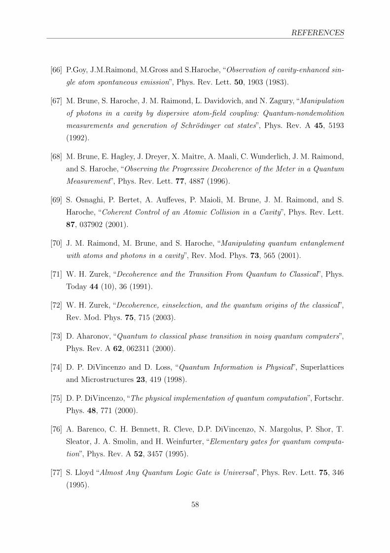
REFERENCES
[66] P.Goy, J.M.Raimond, M.Gross and S.Haroche, “Observation of cavity-enhanced sin-
gle atom spontaneous emission”, Phys. Rev. Lett. 50, 1903 (1983).
[67] M. Brune, S. Haroche, J. M. Raimond, L. Davidovich, and N. Zagury,“Manipulation
of photons in a cavity by dispersive atom-field coupling: Quantum-nondemolition
measurements and generation of Schrodinger cat states”, Phys. Rev. A 45, 5193
(1992).
[68] M. Brune, E. Hagley, J. Dreyer, X. Maitre, A. Maali, C. Wunderlich, J. M. Raimond,
and S. Haroche, “Observing the Progressive Decoherence of the Meter in a Quantum
Measurement”, Phys. Rev. Lett. 77, 4887 (1996).
[69] S. Osnaghi, P. Bertet, A. Auffeves, P. Maioli, M. Brune, J. M. Raimond, and S.
Haroche, “Coherent Control of an Atomic Collision in a Cavity”, Phys. Rev. Lett.
87, 037902 (2001).
[70] J. M. Raimond, M. Brune, and S. Haroche, “Manipulating quantum entanglement
with atoms and photons in a cavity”, Rev. Mod. Phys. 73, 565 (2001).
[71] W. H. Zurek, “Decoherence and the Transition From Quantum to Classical”, Phys.
Today 44 (10), 36 (1991).
[72] W. H. Zurek, “Decoherence, einselection, and the quantum origins of the classical”,
Rev. Mod. Phys. 75, 715 (2003).
[73] D. Aharonov, “Quantum to classical phase transition in noisy quantum computers”,
Phys. Rev. A 62, 062311 (2000).
[74] D. P. DiVincenzo and D. Loss, “Quantum Information is Physical”, Superlattices
and Microstructures 23, 419 (1998).
[75] D. P. DiVincenzo,“The physical implementation of quantum computation”, Fortschr.
Phys. 48, 771 (2000).
[76] A. Barenco, C. H. Bennett, R. Cleve, D.P. DiVincenzo, N. Margolus, P. Shor, T.
Sleator, J. A. Smolin, and H. Weinfurter, “Elementary gates for quantum computa-
tion”, Phys. Rev. A 52, 3457 (1995).
[77] S. Lloyd “Almost Any Quantum Logic Gate is Universal”, Phys. Rev. Lett. 75, 346
(1995).
58
REFERENCES
[78] Q. A. Turchette, C. J. Hood, W. Lange, H. Mabuchi, and H. J. Kimble, “Mea-
surement of conditional phase shifts for quantum logic”, Phys. Rev. Lett. 75, 4710
(1995).
[79] R. Hanson, L. P. Kouwenhoven, J. R. Petta, S. Tarucha, and L. M. K. Vandersypen,
“Spins in few-electron quantum dots”, Rev. Mod. Phys. 79, 1217 (2007).
[80] S. Amasha, K. MacLean, I. P. Radu, D. M. Zumbuh, M. A. Kastner, M. P. Hanson,
and A. C. Gossard, “Electrical Control of Spin Relaxation in a Quantum Dot”, Phys.
Rev. Lett. 100, 046803 (2008).
[81] J. R. Petta, A. C. Johnson, J. M. Taylor, E. A. Laird, A. Yacoby, M. D. Lukin, C.
M. Marcus, M. P. Hanson, and A. C. Gossard, “Coherent Manipulation of Coupled
Electron Spins in Semiconductor Quantum Dots”, Science 309, 2180 (2005).
[82] J. M. Elzerman, R. Hanson, L. H. Willems van Beveren, B. Witkamp, L. M. K.
Vandersypen, and L. P. Kouwenhoven,“Single-shot read-out of an individual electron
spin in a quantum dot”, Nature (London) 430, 431 (2004).
[83] R. Hanson, L. H. Willems van Beveren, I. T. Vink, J. M. Elzerman, W. J. M. Naber,
F. H. L. Koppens, L. P. Kouwenhoven, and L. M. K. Vandersypen, “Single-Shot
Readout of Electron Spin States in a Quantum Dot Using Spin-Dependent Tunnel
Rates”, Phys. Rev. Lett. 94, 196802 (2005).
[84] T. Meunier, I. T. Vink, L. H. Willems van Beveren, F. H. L. Koppens, H. P. Tranitz,
W. Wegscheider, L. P. Kouwenhoven, and L. M. K. Vandersypen, “Nondestructive
measurement of electron spins in a quantum dot”, Phys. Rev. B 74, 195303 (2006).
[85] F. H. L. Koppens, C. Buizert, K. J. Tielrooij, I. T. Vink, K. C. Nowack, T. Meunier,
L. P. Kouwenhoven, and L. M. K. Vandersypen, “Driven coherent oscillations of a
single electron spin in a quantum dot”, Nature (London) 442, 766 (2006).
[86] A. Morello, J. J. Pla, F. A. Zwanenburg, K. W. Chan, K. Y. Tan, H. Huebl, M.
Mottonen, C. D. Nugroho, C. Yang, J. A. van Donkelaar, A. D. C. Alves, D. N.
Jamieson, C. C. Escott, L. C. L. Hollenberg, R. G. Clark, and A. S. Dzurak, “Single-
shot readout of an electron spin in silicon”, Nature (London) 467, 687 (2010).
[87] A. J. Ramsay, S. J. Boyle, R. S. Kolodka, J. B. B. Oliveira, J. Skiba-Szymanska,
H. Y. Liu, M. Hopkinson, A. M. Fox, and M. S. Skolnick “Fast Optical Preparation,
59
REFERENCES
Control, and Readout of a Single Quantum Dot Spin”, Phys. Rev. Lett. 100, 197401
(2008).
[88] D. Press, T. D. Ladd, B. Zhang, and Y. Yamamoto, “Complete quantum control of
a single quantum dot spin using ultrafast optical pulses”, Nature (LONDON) 456,
218 (2008).
[89] K. C. Nowack, F. H. L. Koppens, Yu. V. Nazarov, and L. M. K. Vandersypen,
“Coherent Control of a Single Electron Spin with Electric Fields”, Science 318, 1430
(2007).
[90] S. Nadj-Perge, S. M. Frolov, E. P. A. M. Bakkers and L. P. Kouwenhoven,“Spin-orbit
qubit in a semiconductor nanowire”, Nature (London) 468, 1084 (2010).
[91] S. Nadj-Perge, V. S. Pribiag, J. W. G. van den Berg, K. Zuo1, S. R. Plissard, E. P.
A. M. Bakkers, S. M. Frolov, and L. P. Kouwenhoven, “Spectroscopy of Spin-Orbit
Quantum Bits in Indium Antimonide Nanowires”, Phys. Rev. Lett. 108, 166801
(2012).
[92] R. Hanson and D. D. Awschalom, “Coherent manipulation of single spins in semi-
conductors”, Nature (London) 453, 1043 (2008).
[93] R. Brunner, Y.-S. Shin, T. Obata, M. Pioro-Ladriere, T. Kubo, K. Yoshida, T.
Taniyama, Y. Tokura, and S. Tarucha, “Two-Qubit Gate of Combined Single-Spin
Rotation and Interdot Spin Exchange in a Double Quantum Dot”, Phys. Rev. Lett.
107, 146801 (2011).
[94] K. C. Nowack, M. Shafiei, M. Laforest, G. E. D. K. Prawiroatmodjo, L. R. Schreiber,
C. Reichl, W. Wegscheider, L. M. K. Vandersypen, “Single-Shot Correlations and
Two-Qubit Gate of Solid-State Spins”, Science 333, 1269 (2011).
[95] D. D. Awschalom , L. C. Bassett, A. S. Dzurak, E. L. Hu, and J. R. Petta,“Quantum
Spintronics: Engineering and Manipulating Atom-Like Spins in Semiconductors”
Science 339, 1174 (2013).
[96] L. M. K. Vandersypen, M. Steffen, G. Breyta, C. S. Yannoni, M. H. Sherwood, and
I. L. Chuang, “Experimental realization of Shor’s quantum factoring algorithm using
nuclear magnetic resonance”, Nature (London) 414, 883 (2001).
60
REFERENCES
[97] C.-Y. Lu, D. E. Browne, T. Yang, and J.-W. Pan, “Demonstration of a Compiled
Version of Shor’s Quantum Factoring Algorithm Using Photonic Qubits”, Phys. Rev.
Lett. 99, 250504 (2007).
[98] B. P. Lanyon, T. J. Weinhold, N. K. Langford, M. Barbieri, D. F. V. James, A.
Gilchrist, and A. G. White, “Experimental Demonstration of a Compiled Version of
Shor’s Algorithm with Quantum Entanglement”, Phys. Rev. Lett. 99, 250505 (2007).
[99] E. Lucero, R. Barends, Y. Chen, J. Kelly, M. Mariantoni, A. Megrant, P. O’Malley,
D. Sank, A. Vainsencher, J. Wenner, T. White, Y. Yin, A. N. Cleland, and John M.
Martinis, “Computing prime factors with a Josephson phase qubit quantum proces-
sor”, Nature Physics 8, 719 (2012).
[100] E. Martin-Lopez, A. Laing, T. Lawson, R. Alvarez, X.-Q. Zhou, and J. L. O’Brien,
“Experimental realization of Shor’s quantum factoring algorithm using qubit recy-
cling”, Nature Photonics 6, 773 (2012).
[101] D. P. DiVincenzo, D. Bacon, J. Kempe, G. Burkard, and K. B. Whaley, “Universal
quantum computation with the exchange interaction”, Nature (London) 408, 339
(2000).
[102] V. N. Golovach, M. Borhani, and D. Loss, “Electric-dipole-induced spin resonance
in quantum dots”, Phys. Rev. B 74, 165319 (2006).
[103] S. Debald and C. Emary, “Spin-Orbit-Driven Coherent Oscillations in a Few-
Electron Quantum Dot”, Phys. Rev. Lett. 94, 226803 (2005).
[104] C. Flindt, A. S. Sorensen, and K. Flensberg, “Spin-Orbit Mediated Control of Spin
Qubits”, Phys. Rev. Lett. 97, 240501 (2006).
[105] I. A. Merkulov, Al. L. Efros, and M. Rosen, “Electron spin relaxation by nuclei in
semiconductor quantum dots”, Phys. Rev. B 65, 205309 (2002).
[106] A. V. Khaetskii, D. Loss, and L. Glazman, “Electron Spin Decoherence in Quantum
Dots due to Interaction with Nuclei”, Phys. Rev. Lett. 88, 186802 (2002).
[107] L. Cywinski, W. M. Witzel, and S. Das Sarma, “Electron Spin Dephasing due to
Hyperfine Interactions with a Nuclear Spin Bath”, Phys. Rev. Lett. 102, 057601
(2009).
61
REFERENCES
[108] W. A. Coish and J. Baugh, “Nuclear spins in nanostructures”, Phys. Status Solidi
B 246, 2203 (2009).
[109] J. Fischer and D. Loss, “Dealing with Decoherence”, Science 324, 1277 (2009).
[110] H. Bluhm, S. Foletti, I. Neder, M. Rudner, D. Mahalu, V. Umansky, A. Yacoby,
“Dephasing time of GaAs electron-spin qubits coupled to a nuclear bath exceeding
200 us”, Nature Phys. 7, 109 (2010).
[111] G. Burkard, “Positively spin coherent”, Nature Materials 7, 100 (2008).
[112] M. H. Kolodrubetz, J. R. Petta, “Coherent holes in a semiconductor quantum dot”,
Science 325, 42 (2009).
[113] A. Tartakovskii, “Holes avoid decoherence”, Nature Photonics 5, 647 (2011).
[114] J. Fischer, W. A. Coish, D. V. Bulaev, and D. Loss, “Spin decoherence of a heavy
hole coupled to nuclear spins in a quantum dot”, Phys. Rev. B 78, 155329 (2008).
[115] C. Testelin, F. Bernardot, B. Eble, and M. Chamarro, “Hole-spin dephasing time
associated with hyperfine interaction in quantum dots”, Phys. Rev. B 79, 195440
(2009).
[116] B. Eble, C. Testelin, P. Desfonds, F. Bernardot, A. Balocchi, T. Amand, A. Miard, A.
Lemaitre, X. Marie, and M. Chamarro, “Hole-Nuclear Spin Interaction in Quantum
Dots”, Phys. Rev. Lett. 102, 146601 (2009).
[117] P. Fallahi, S. T. Yilmaz, and A. Imamoglu,“Measurement of a Heavy-Hole Hyperfine
Interaction in InGaAs Quantum Dots Using Resonance Fluorescence”, Phys. Rev.
Lett. 105, 257402 (2010).
[118] P. Desfonds, B. Eble, F. Fras, C. Testelin, F. Bernardot, M. Chamarro, B. Urbaszek,
T. Amand, X. Marie, J.-M. Gerard, V. Thierry-Mieg, A. Miard, and A. Lemaitre,
“Electron and hole spin cooling efficiency in InAs quantum dots: The role of nuclear
field”, Appl. Phys. Lett. 96, 172108 (2010).
[119] E. A. Chekhovich, A. B. Krysa, M. S. Skolnick, and A. I. Tartakovskii, “Direct
Measurement of the Hole-Nuclear Spin Interaction in Single InP/GaInP Quantum
Dots Using Photoluminescence Spectroscopy”, Phys. Rev. Lett. 106, 027402 (2011).
62
REFERENCES
[120] Z. K. Keane, M. C. Godfrey, J. C. H. Chen, S. Fricke, O. Klochan, A. M. Burke,
A. P. Micolich, H. E. Beere, D. A. Ritchie, K. V. Trunov, D. Reuter, A. D. Wieck,
and A. R. Hamilton, “Resistively Detected Nuclear Magnetic Resonance in n- and
p-Type GaAs Quantum Point Contacts”, Nano Lett. 11, 3147 (2011).
[121] K. Yano and D. K. Ferry, “Single-electron solitons” Superlattices Microstruct. 11,
61 (1991).
[122] S. Bednarek, B. Szafran, and K. Lis, “Electron soliton in semiconductor nanostruc-
tures” Phys. Rev. B 72, 075319 (2005).
[123] S. Bednarek, B. Szafran, K. Lis, “Self-focusing of a quantum-well confined electron
wave packet interacting with a metal plate”, Phys. Stat. Sol. (b) 243 2811 (2006).
[124] S. Bednarek, B. Szafran, “Energy dissipation of electron solitons in a quantum well”
Phys. Rev. B 73, 155318 (2006).
[125] S. Bednarek, B. Szafran, R. J. Dudek, K. Lis, “Induced quantum dots and wires:
Electron storage and delivery” Phys. Rev. Lett. 100, 126805 (2008).
[126] S. Bednarek, B. Szafran,“Spin rotations induced by an electron running in closed tra-
jectories in gated semiconductor nanodevices” Phys. Rev. Lett. 101, 216805 (2008).
[127] S. Bednarek, B. Szafran,“Gated combo nanodevice for sequential operations on single
electron spin”, Nanotechnology 20, 065402 (2009).
[128] G. Dresselhaus, “Spin-Orbit Coupling Effects in Zinc Blende Structures”, Phys. Rev.
100, 580 (1955).
[129] E. I. Rashba, Fiz. Tverd. Tela (Leningrad) 2, 1224 (1960) [Sov. Phys. Solid State 2,
1109 (1960)].
[130] Y.A. Bychkov and E.I. Rashba, “Oscillatory effects and the magnetic susceptibility
of carriers in inversion layers”, J. Phys. C 17, 6039 (1984).
[131] S. Bednarek, K. Lis, B. Szafran, “Quantum dot defined in a two-dimensional elec-
tron gas at n-AlGaAs/GaAs heterojunction: Simulation of electrostatic potential and
charging properties” Phys. Rev. B 77, 115320 (2008).
63
REFERENCES
[132] J. M. Elzerman, R. Hanson, L. H. Willems van Beveren, L. M. K. Vandersypen, and
L. P. Kouwenhoven, “Excited-state spectroscopy on a nearly closed quantum dot via
charge detection”, Appl. Phys. Lett. 84, 4617 (2004).
[133] S. Cortez, O. Krebs, S. Laurent, M. Senes, X. Marie, P. Voisin, R. Ferreira, G.
Bastard, J. M. Gerard, and T. Amand, “Optically Driven Spin Memory in n-Doped
InAs-GaAs Quantum Dots”, Phys. Rev. Lett. 89, 207401 (2002).
[134] A. Shabaev, Al. L. Efros, D. Gammon, and I. A. Merkulov, “Optical readout and ini-
tialization of an electron spin in a single quantum dot”, Phys. Rev. B 68, 201305(R)
(2003).
[135] O. Gywat, H.-A. Engel, D. Loss, R. J. Epstein, F. M. Mendoza, and D. D.
Awschalom,“Optical detection of single-electron spin decoherence in a quantum dot”,
Phys. Rev. B 69, 205303 (2004).
[136] A. S. Bracker, E. A. Stinaff, D. Gammon, M. E. Ware, J. G. Tischler, A. Shabaev,
Al. L. Efros, D. Park, D. Gershoni, V. L. Korenev, and I. A. Merkulov, “Optical
Pumping of the Electronic and Nuclear Spin of Single Charge-Tunable Quantum
Dots”, Phys. Rev. Lett. 94, 047402 (2005).
[137] M. Atature, J. Dreiser, A. Badolato , A. Hogele, K. Karrai, and A. Imamoglu,
“Quantum-Dot Spin-State Preparation with Near-Unity Fidelity”, Science, 312, 551
(2006).
[138] K. Ono , D. G. Austing, Y. Tokura, and S. Tarucha, “Current Rectification by Pauli
Exclusion in a Weakly Coupled Double Quantum Dot System”, Science, 297, 1313
(2002).
[139] A. C. Johnson , J. R. Petta , C. M. Marcus , M. P. Hanson and A. C. Gossard,
“Singlet-triplet spin blockade and charge sensing in a few-electron double quantum
dot”, Phys. Rev. B, 72, 165308 (2005).
[140] S. Datta and B. Das, “Electronic analog of the electrooptic modulator”, Appl. Phys.
Lett. 56, 665 (1990).
[141] J. Schliemann, C. Egues, J, and D. Loss, “Nonballistic Spin-Field-Effect Transistor”,
Phys. Rev. Lett. 90, 146801 (2003).
64
REFERENCES
[142] J.E. Hirsch, “Spin Hall Effect”, Phys. Rev. Lett. 83, 1834 (1999).
[143] M. I. Dyakonov and V. I. Perel’ “Possibility of orientating electron spins with cur-
rent”. Sov. Phys. JETP Lett. 13, 467 (1971).
[144] M.I. Dyakonov and V.I. Perel’. “Current-induced spin orientation of electrons in
semiconductors”. Phys. Lett. A 35 (6) 459 (1971).
[145] Y. Kato, R. C. Myers, A. C. Gossard, D. D. Awschalom “Observation of the Spin
Hall Effect in Semiconductors”, Science 306 1910 (2004).
[146] J. Wunderlich, B. Kaestner, J. Sinova and T. Jungwirth, “Experimental Observation
of the Spin-Hall Effect in a Two-DimensionalSpin-Orbit Coupled Semiconductor
System”, Phys. Rev. Lett. 94 047204 (2005).
[147] J. C. Egues “Spin-Dependent Perpendicular Magnetotransport through a Tunable
ZnSe/Zn1−xMnxSe Heterostructure: A Possible Spin Filter?” Phys. Rev. Lett. 80,
4578 (1998).
[148] M. Field, C. G. Smith, M. Pepper, D. A. Ritchie, J. E. F. Frost, G. A. C. Jones,
and D. G. Hasko, “Measurements of Coulomb blockade with a noninvasive voltage
probe”, Phys. Rev. Lett. 70, 1311 (1993).
[149] D. Heiss, S. Schaeck, H. Huebl, M. Bichler, G. Abstreiter, J. J. Finley, D. V. Bulaev,
and D. Loss, “Observation of extremely slow hole spin relaxation in self-assembled
quantum dots”, Phys. Rev. B 76, 241306 (2007).
[150] B. D. Gerardot, D. Brunner, P. A. Dalgarno, P. Ohberg, S. Seidl, M. Kroner., K.
Karrai, N. G. Stoltz, P. M. Petroff, and R. J. Warburton, “Optical pumping of a
single hole spin in a quantum dot”, Nature (London) 451, 441 (2008).
[151] F. Fras, B. Eble, P. Desfonds, F. Bernardot, C. Testelin, M. Chamarro, A. Miard, and
A. Lemaitre, “Hole-spin initialization and relaxation times in InAs/GaAs quantum
dots”, Phys. Rev. B 84, 125431 (2011).
[152] D. V. Bulaev and D. Loss, “Electric Dipole Spin Resonance for Heavy Holes in
Quantum Dots”, Phys. Rev. Lett. 98, 097202 (2007).
65
REFERENCES
[153] J. C. Budich, D. G. Rothe, E. M. Hankiewicz, and B. Trauzettel, “All-electric qubit
control in heavy hole quantum dots via non-Abelian geometric phases”, Phys. Rev.
B 85, 205425 (2012).
[154] C. Hsieh, R. Cheriton, M. Korkusinski, and P. Hawrylak,“Valence holes as Luttinger
spinor based qubits in quantum dots”, Phys. Rev. B 80, 235320 (2009).
[155] T. Andlauer and P. Vogl, “Electrically controllable g tensors in quantum dot
molecules”, Phys. Rev. B 79, 045307 (2009).
[156] R. Roloff, T. Eissfeller, P. Vogl, and W. Potz, “Electric g tensor control and spin
echo of a hole-spin qubit in a quantum dot molecule”, New J. Phys. 12, 093012
(2010).
[157] K. De Greve, P. L. McMahon, D. Press, T. D. Ladd, D. Bisping, C. Schneider, M.
Kamp, L. Worschech, S. Hofling, A. Forchel, and Y. Yamamoto, “Coherent control
and suppressed nuclear feedback of a single quantum dot hole qubit”, Nature Physics
7, 872 (2011).
[158] A. Greilich, S. G. Carter, D. Kim, A. S. Bracker, and D. Gammon, “Optical control
of one and two hole spins in interacting quantum dots”, Nature Photonics 5, 702
(2011).
[159] T. M. Godden, J. H. Quilter, A. J. Ramsay, Yanwen Wu, P. Brereton, S. J. Boyle,
I. J. Luxmoore, J. Puebla-Nunez, A. M. Fox, and M. S. Skolnick, “Coherent Optical
Control of the Spin of a Single Hole in an InAs/GaAs Quantum Dot”, Phys. Rev.
Lett. 108, 017402 (2012).
[160] K. Muller, A. Bechtold, C. Ruppert, C. Hautmann, J. S. Wildmann, T. Kaldewey,
M. Bichler, H. J. Krenner, G. Abstreiter, M. Betz, and J. J. Finley, “High-fidelity
optical preparation and coherent Larmor precession of a single hole in an (In,Ga)As
quantum dot molecule”, Phys. Rev. B 85, 241306 (2012).
[161] B. Eble, P. Desfonds, F. Fras, F. Bernardot, C. Testelin, M. Chamarro, A. Miard,
and A. Lemaitre, “Hole and trion spin dynamics in quantum dots under excitation
by a train of circularly polarized pulses”, Phys. Rev. B 81, 045322 (2010).
66
REFERENCES
[162] F. Fras, B. Eble, F. Bernardot, C. Testelin, M. Chamarro, A. Miard, and A.
Lemaitre, “Optical pumping and reversal of hole spin in InAs/GaAs quantum dots”,
Appl. Phys. Lett. 100, 012104 (2012).
[163] A. J. Ramsay, S. J. Boyle, R. S. Kolodka, J. B. B. Oliveira, J. Skiba-Szymanska, H.
Y. Liu, M. Hopkinson, A. M. Fox, and M. S. Skolnick, “Fast Optical Preparation,
Control, and Readout of a Single Quantum Dot Spin”, Phys. Rev. Lett. 100, 197401
(2008).
[164] T. M. Godden, J. H. Quilter, A. J. Ramsay, Y. W. Wu, P. Brereton, I. J. Luxmoore,
J. Puebla, A. M. Fox, and M. S. Skolnick, “Fast preparation of a single-hole spin in
an InAs/GaAs quantum dot in a Voigt-geometry magnetic field”, Phys. Rev. B 85,
155310 (2012).
[165] V. S. Pribiag, S. Nadj-Perge, S. M. Frolov, J. W. G. van den Berg, I. van Weperen,
S. R. Plissard, E. P. A. M. Bakkers, and L. P. Kouwenhoven, “Electrical control of
single hole spins in nanowire quantum dots”, Nature Nanotechnology 8, 170 (2013).
67