
Cienkowarstwowe ogniwo słoneczneadam.mech.pw.edu.pl/~marzan/9_Pl_Eng.pdfStrona 1 Politechnika...
32
Strona 1 Politechnika Warszawska Do użytku wewnętrznego Wydzial Fizyki Laboratorium Fizyki II p. Malgorzata Igalson, Jan Ulaczyk Cienkowarstwowe ogniwo sloneczne 1.Promieniowanie sloneczne Slońce jest najważniejszym źródlem energii na Ziemi: do powierzchni atmosfery w poludnie na równiku dociera moc równa stalej slonecznej P=1,3661 kW/m 2 . Wartość tej mocy przyjęlo się oznaczać jako A.M. (air mass) 0. Patrz rys.1. Energia promieniowania slonecznego jest częściowo absorbowana przez atmosferę, tak więc do powierzchni dociera ok. 73 % (A.M. 1). Rys. 1. Definicja oznaczenia A.M. Wartość ta odpowiada mocy, która najkrótszą drogą (prostopadle) osiąga powierzchnię Ziemi – czyli w poludnie na równiku. Dla innych szerokości geograficznych ilość energii docierającej do powierzchni będzie zależala od kąta, pod którym to promieniowanie pada na danej szerokości geograficznej i można latwo ją obliczyć z relacji: AMX=AM1/cos φ (1) W naszej szerokości geograficznej za standard przyjmuje się wartość mocy odpowiadającej ok. A.M. 1.5 równą 800 W/m 2 . Wydajności ogniw slonecznych są podawane wlaśnie dla tej standardowej mocy promieniowania. Na obszarze Polski calkowita wartość energii slonecznej docierającej średnio w ciągu roku wynosi ok. 1000 kWh/m 2 .
-
Upload
truongphuc -
Category
Documents
-
view
213 -
download
0
Transcript of Cienkowarstwowe ogniwo słoneczneadam.mech.pw.edu.pl/~marzan/9_Pl_Eng.pdfStrona 1 Politechnika...

Strona 1
Politechnika Warszawska Do użytku wewnętrznego Wydział Fizyki Laboratorium Fizyki II p. Małgorzata Igalson, Jan Ulaczyk
Cienkowarstwowe ogniwo słoneczne 1.Promieniowanie słoneczne
Słońce jest najważniejszym źródłem energii na Ziemi: do powierzchni atmosfery w południe na równiku dociera moc równa stałej słonecznej P=1,3661 kW/m2. Wartość tej mocy przyjęło się oznaczać jako A.M. (air mass) 0. Patrz rys.1. Energia promieniowania słonecznego jest częściowo absorbowana przez atmosferę, tak więc do powierzchni dociera ok. 73 % (A.M. 1).
Rys. 1. Definicja oznaczenia A.M.
Wartość ta odpowiada mocy, która najkrótszą drogą (prostopadle) osiąga powierzchnię Ziemi – czyli w południe na równiku. Dla innych szerokości geograficznych ilość energii docierającej do powierzchni będzie zależała od kąta, pod którym to promieniowanie pada na danej szerokości geograficznej i można łatwo ją obliczyć z relacji:
AMX=AM1/cos φ (1)
W naszej szerokości geograficznej za standard przyjmuje się wartość mocy odpowiadającej ok. A.M. 1.5 równą 800 W/m2. Wydajności ogniw słonecznych są podawane właśnie dla tej standardowej mocy promieniowania. Na obszarze Polski całkowita wartość energii słonecznej docierającej średnio w ciągu roku wynosi ok. 1000 kWh/m2.
Strona 2
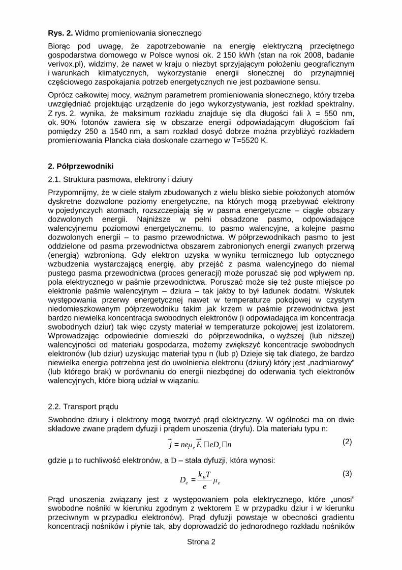
Rys. 2. Widmo promieniowania słonecznego
Biorąc pod uwagę, że zapotrzebowanie na energię elektryczną przeciętnego gospodarstwa domowego w Polsce wynosi ok. 2 150 kWh (stan na rok 2008, badanie verivox.pl), widzimy, że nawet w kraju o niezbyt sprzyjającym położeniu geograficznym i warunkach klimatycznych, wykorzystanie energii słonecznej do przynajmniej częściowego zaspokajania potrzeb energetycznych nie jest pozbawione sensu.
Oprócz całkowitej mocy, ważnym parametrem promieniowania słonecznego, który trzeba uwzględniać projektując urządzenie do jego wykorzystywania, jest rozkład spektralny. Z rys. 2. wynika, że maksimum rozkładu znajduje się dla długości fali λ = 550 nm, ok. 90% fotonów zawiera się w obszarze energii odpowiadającym długościom fali pomiędzy 250 a 1540 nm, a sam rozkład dosyć dobrze można przybliżyć rozkładem promieniowania Plancka ciała doskonale czarnego w T=5520 K.
2. Półprzewodniki
2.1. Struktura pasmowa, elektrony i dziury
Przypomnijmy, że w ciele stałym zbudowanych z wielu blisko siebie położonych atomów dyskretne dozwolone poziomy energetyczne, na których mogą przebywać elektrony w pojedynczych atomach, rozszczepiają się w pasma energetyczne – ciągłe obszary dozwolonych energii. Najniższe w pełni obsadzone pasmo, odpowiadające walencyjnemu poziomowi energetycznemu, to pasmo walencyjne, a kolejne pasmo dozwolonych energii – to pasmo przewodnictwa. W półprzewodnikach pasmo to jest oddzielone od pasma przewodnictwa obszarem zabronionych energii zwanych przerwą (energią) wzbronioną. Gdy elektron uzyska w wyniku termicznego lub optycznego wzbudzenia wystarczającą energię, aby przejść z pasma walencyjnego do niemal pustego pasma przewodnictwa (proces generacji) może poruszać się pod wpływem np. pola elektrycznego w paśmie przewodnictwa. Poruszać może się też puste miejsce po elektronie paśmie walencyjnym – dziura – tak jakby to był ładunek dodatni. Wskutek występowania przerwy energetycznej nawet w temperaturze pokojowej w czystym niedomieszkowanym półprzewodniku takim jak krzem w paśmie przewodnictwa jest bardzo niewielka koncentracja swobodnych elektronów (i odpowiadająca im koncentracja swobodnych dziur) tak więc czysty materiał w temperaturze pokojowej jest izolatorem. Wprowadzając odpowiednie domieszki do półprzewodnika, o wyższej (lub niższej) walencyjności od materiału gospodarza, możemy zwiększyć koncentracje swobodnych elektronów (lub dziur) uzyskując materiał typu n (lub p) Dzieje się tak dlatego, że bardzo niewielka energia potrzebna jest do uwolnienia elektronu (dziury) który jest „nadmiarowy” (lub którego brak) w porównaniu do energii niezbędnej do oderwania tych elektronów walencyjnych, które biorą udział w wiązaniu.
2.2. Transport prądu
Swobodne dziury i elektrony mogą tworzyć prąd elektryczny. W ogólności ma on dwie składowe zwane prądem dyfuzji i prądem unoszenia (dryfu). Dla materiału typu n:
neDEneµj ee ∇+= (2)
gdzie µ to ruchliwość elektronów, a D – stała dyfuzji, która wynosi:
e
Be µ
e
TkD =
(3)
Prąd unoszenia związany jest z występowaniem pola elektrycznego, które „unosi” swobodne nośniki w kierunku zgodnym z wektorem E w przypadku dziur i w kierunku przeciwnym w przypadku elektronów). Prąd dyfuzji powstaje w obecności gradientu koncentracji nośników i płynie tak, aby doprowadzić do jednorodnego rozkładu nośników
Strona 3
w objętości półprzewodnika. Ruchliwość definiujemy jako prędkość dryfu na jednostkę pola elektrycznego:
µ=vd/E (4)
i jest ona miarą zdolności poruszanie się swobodnych nośników w kierunku pola: im więcej niedoskonałości (defektów, drgań sieci krystalicznej) tym jest ona mniejsza. (więcej informacji w instrukcji do ćw. 12).
2.3. Generacja i rekombinacja
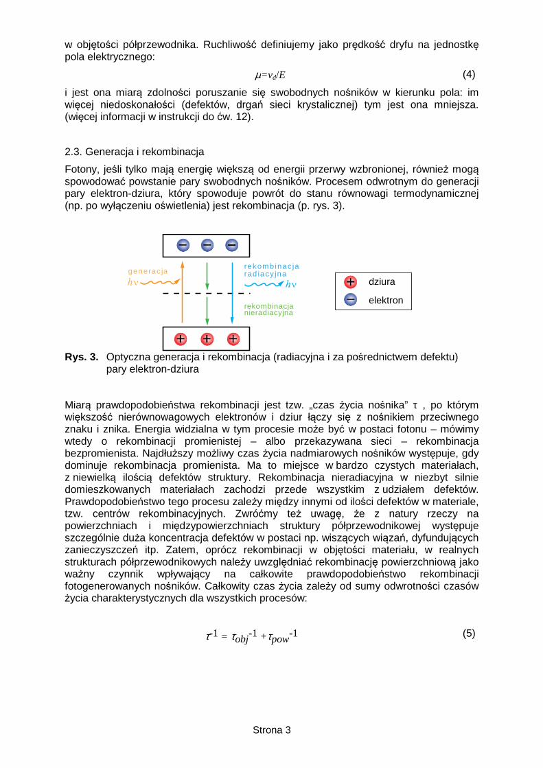
Fotony, jeśli tylko mają energię większą od energii przerwy wzbronionej, również mogą spowodować powstanie pary swobodnych nośników. Procesem odwrotnym do generacji pary elektron-dziura, który spowoduje powrót do stanu równowagi termodynamicznej (np. po wyłączeniu oświetlenia) jest rekombinacja (p. rys. 3).
generac jarekom b inac jarad iacy jna
rekombinacjanieradiacyjna
elektron
dziura
Rys. 3. Optyczna generacja i rekombinacja (radiacyjna i za pośrednictwem defektu)
pary elektron-dziura
Miarą prawdopodobieństwa rekombinacji jest tzw. „czas życia nośnika” τ , po którym większość nierównowagowych elektronów i dziur łączy się z nośnikiem przeciwnego znaku i znika. Energia widzialna w tym procesie może być w postaci fotonu – mówimy wtedy o rekombinacji promienistej – albo przekazywana sieci – rekombinacja bezpromienista. Najdłuższy możliwy czas życia nadmiarowych nośników występuje, gdy dominuje rekombinacja promienista. Ma to miejsce w bardzo czystych materiałach, z niewielką ilością defektów struktury. Rekombinacja nieradiacyjna w niezbyt silnie domieszkowanych materiałach zachodzi przede wszystkim z udziałem defektów. Prawdopodobieństwo tego procesu zależy między innymi od ilości defektów w materiale, tzw. centrów rekombinacyjnych. Zwróćmy też uwagę, że z natury rzeczy na powierzchniach i międzypowierzchniach struktury półprzewodnikowej występuje szczególnie duża koncentracja defektów w postaci np. wiszących wiązań, dyfundujących zanieczyszczeń itp. Zatem, oprócz rekombinacji w objętości materiału, w realnych strukturach półprzewodnikowych należy uwzględniać rekombinację powierzchniową jako ważny czynnik wpływający na całkowite prawdopodobieństwo rekombinacji fotogenerowanych nośników. Całkowity czas życia zależy od sumy odwrotności czasów życia charakterystycznych dla wszystkich procesów:
τ-1 = τobj-1 +τpow
-1 (5)
Strona 4
3. Efekt fotowoltaiczny w zł ączu pn
3.1. Złącze pn
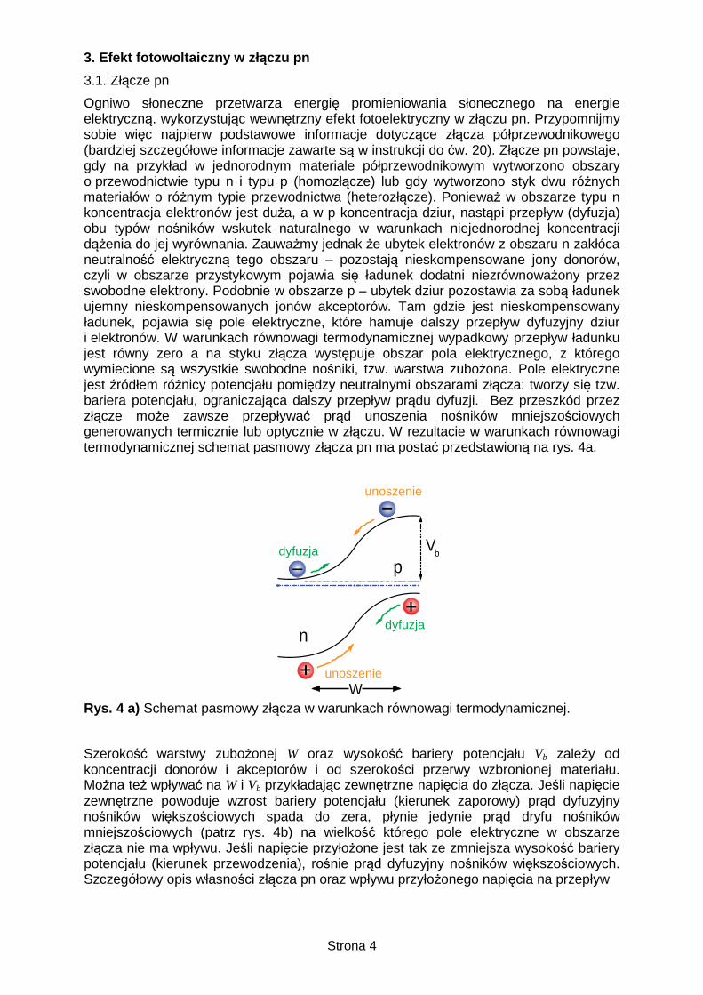
Ogniwo słoneczne przetwarza energię promieniowania słonecznego na energie elektryczną. wykorzystując wewnętrzny efekt fotoelektryczny w złączu pn. Przypomnijmy sobie więc najpierw podstawowe informacje dotyczące złącza półprzewodnikowego (bardziej szczegółowe informacje zawarte są w instrukcji do ćw. 20). Złącze pn powstaje, gdy na przykład w jednorodnym materiale półprzewodnikowym wytworzono obszary o przewodnictwie typu n i typu p (homozłącze) lub gdy wytworzono styk dwu różnych materiałów o różnym typie przewodnictwa (heterozłącze). Ponieważ w obszarze typu n koncentracja elektronów jest duża, a w p koncentracja dziur, nastąpi przepływ (dyfuzja) obu typów nośników wskutek naturalnego w warunkach niejednorodnej koncentracji dążenia do jej wyrównania. Zauważmy jednak że ubytek elektronów z obszaru n zakłóca neutralność elektryczną tego obszaru – pozostają nieskompensowane jony donorów, czyli w obszarze przystykowym pojawia się ładunek dodatni niezrównoważony przez swobodne elektrony. Podobnie w obszarze p – ubytek dziur pozostawia za sobą ładunek ujemny nieskompensowanych jonów akceptorów. Tam gdzie jest nieskompensowany ładunek, pojawia się pole elektryczne, które hamuje dalszy przepływ dyfuzyjny dziur i elektronów. W warunkach równowagi termodynamicznej wypadkowy przepływ ładunku jest równy zero a na styku złącza występuje obszar pola elektrycznego, z którego wymiecione są wszystkie swobodne nośniki, tzw. warstwa zubożona. Pole elektryczne jest źródłem różnicy potencjału pomiędzy neutralnymi obszarami złącza: tworzy się tzw. bariera potencjału, ograniczająca dalszy przepływ prądu dyfuzji. Bez przeszkód przez złącze może zawsze przepływać prąd unoszenia nośników mniejszościowych generowanych termicznie lub optycznie w złączu. W rezultacie w warunkach równowagi termodynamicznej schemat pasmowy złącza pn ma postać przedstawioną na rys. 4a.
unoszenie
dyfuzja
unoszenie
dyfuzja
n
pV
b
W Rys. 4 a) Schemat pasmowy złącza w warunkach równowagi termodynamicznej.
Szerokość warstwy zubożonej W oraz wysokość bariery potencjału Vb zależy od koncentracji donorów i akceptorów i od szerokości przerwy wzbronionej materiału. Można też wpływać na W i Vb przykładając zewnętrzne napięcia do złącza. Jeśli napięcie zewnętrzne powoduje wzrost bariery potencjału (kierunek zaporowy) prąd dyfuzyjny nośników większościowych spada do zera, płynie jedynie prąd dryfu nośników mniejszościowych (patrz rys. 4b) na wielkość którego pole elektryczne w obszarze złącza nie ma wpływu. Jeśli napięcie przyłożone jest tak ze zmniejsza wysokość bariery potencjału (kierunek przewodzenia), rośnie prąd dyfuzyjny nośników większościowych. Szczegółowy opis własności złącza pn oraz wpływu przyłożonego napięcia na przepływ
Strona 5
prądu zawarty jest w instrukcji do ćw. 20. W ogólnym przypadku zależność prądu od napięcia w złączu ma postać:
)
TAk
eV(JI
Bodark 1exp −
= (6)
−
=Tk
eEJJ
B
aooo exp
(7)
gdzie współczynniki A (współczynnik idealności złącza, i Io (prąd nasycenia) zależą od dominującego mechanizmu transportu w złączu (patrz tabela 1.)
Tabela 1. Wartości współczynnika idealności i energii aktywacji prądu nasycenia a współczynniki charakterystyki I-V
Mechanizm transportu A Ea
dyfuzja 1 Eg
Rekombinacja w objętości absorbera 1<A<2 AEa=Eg
Rekombinacja z udziałem stanów na interfejsie 1<A<2 Ea=Vb
j.w. z udziałem tunelowania do tych stanów A>2 Ea<Vb
3.2. Efekt fotowoltaiczny
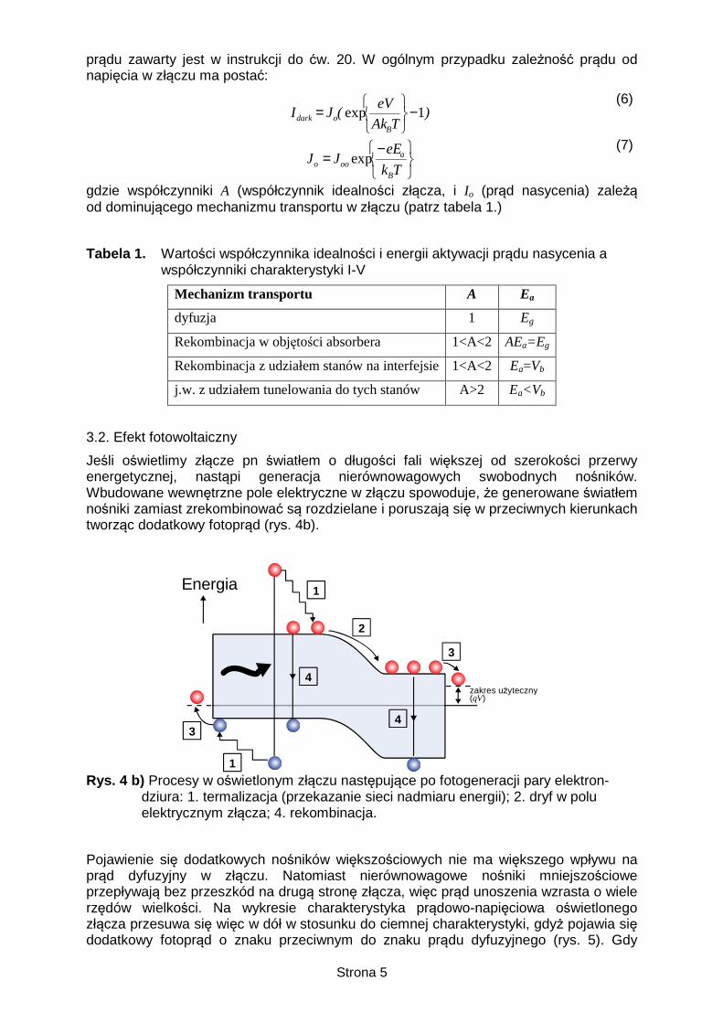
Jeśli oświetlimy złącze pn światłem o długości fali większej od szerokości przerwy energetycznej, nastąpi generacja nierównowagowych swobodnych nośników. Wbudowane wewnętrzne pole elektryczne w złączu spowoduje, że generowane światłem nośniki zamiast zrekombinować są rozdzielane i poruszają się w przeciwnych kierunkach tworząc dodatkowy fotoprąd (rys. 4b).
Energia
zakres użyteczny(qV)
1
2
3
4
4
1
3
Rys. 4 b) Procesy w oświetlonym złączu następujące po fotogeneracji pary elektron-
dziura: 1. termalizacja (przekazanie sieci nadmiaru energii); 2. dryf w polu elektrycznym złącza; 4. rekombinacja.
Pojawienie się dodatkowych nośników większościowych nie ma większego wpływu na prąd dyfuzyjny w złączu. Natomiast nierównowagowe nośniki mniejszościowe przepływają bez przeszkód na drugą stronę złącza, więc prąd unoszenia wzrasta o wiele rzędów wielkości. Na wykresie charakterystyka prądowo-napięciowa oświetlonego złącza przesuwa się więc w dół w stosunku do ciemnej charakterystyki, gdyż pojawia się dodatkowy fotoprąd o znaku przeciwnym do znaku prądu dyfuzyjnego (rys. 5). Gdy
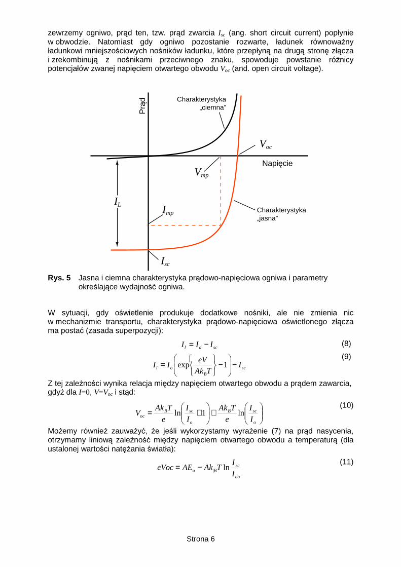
Strona 6
zewrzemy ogniwo, prąd ten, tzw. prąd zwarcia Isc (ang. short circuit current) popłynie w obwodzie. Natomiast gdy ogniwo pozostanie rozwarte, ładunek równoważny ładunkowi mniejszościowych nośników ładunku, które przepłyną na drugą stronę złącza i zrekombinują z nośnikami przeciwnego znaku, spowoduje powstanie różnicy potencjałów zwanej napięciem otwartego obwodu Voc (and. open circuit voltage).
Napięcie
Prą
d
Charakterystyka„jasna”
Charakterystyka„ciemna”
IL
Voc
Vmp
Imp
Isc
Rys. 5 Jasna i ciemna charakterystyka prądowo-napięciowa ogniwa i parametry określające wydajność ogniwa.
W sytuacji, gdy oświetlenie produkuje dodatkowe nośniki, ale nie zmienia nic w mechanizmie transportu, charakterystyka prądowo-napięciowa oświetlonego złącza ma postać (zasada superpozycji):
scdl III −= (8)
sc
Bol I
TAk
eVII −
−
= 1exp (9)
Z tej zależności wynika relacja między napięciem otwartego obwodu a prądem zawarcia, gdyż dla I=0, V=Voc i stąd:
≅
+=
o
scB
o
scBoc I
I
e
TAk
I
I
e
TAkV ln1ln
(10)
Możemy również zauważyć, że jeśli wykorzystamy wyrażenie (7) na prąd nasycenia, otrzymamy liniową zależność między napięciem otwartego obwodu a temperaturą (dla ustalonej wartości natężania światła):
oo
scBa I
ITAkAEeVoc ln|−= (11)

Strona 7
4. Wydajno ść ogniwa
Od wartości parametrów Isc i Voc zależy wydajność ogniwa. Zauważmy bowiem, że wydajność konwersji fotowoltaicznej określa stosunek maksymalnej mocy wytwarzanej w ogniwie do mocy promieniowania padającego na to ogniwo:
in
mpmp
P
VI=η
(12)
Przyjęto, że maksymalną moc wyraża się poprzez tzw. współczynnik wypełnienia FF (patrz Rys. 5)
ocsc
mpmp
VI
VIFF =
(13)
skąd wynika, że:
in
ocsc
P
FFVI=η (14)
Nominalna wydajność konwersji ogniwa jest określana dla standartowych warunków oświetlania i temperatury: 1000 W/m2 (A.M.1.5) przy T=25°C. W tabeli 2. podano rekordowe wartości parametrów dla różnych ogniw.
Tabela 2. Maksymalne wydajności ogniw słonecznych różnego typu.
Ef f.
( %)
Voc
(V)
Js c
(mA/c m2)
FF
(%)
Si-c 2 4.7 0 .70 6 42 .2 82.8
Si-µµµµc 1 9.8 0 .65 4 38 .1 79.5
GaAs-c 2 4.9 0 .87 8 29 .3 85.4 a-Si (m odule) 1 2.0 1 2.5 1.3 73.5 GaAs (thin film) 2 3.3 1 .01 1 27 .6 83.8 C IGS 19.8 0.669 35.7 7 7.0 CIGS ( module ) 16.6 2.643 8.3 5 7 5.1 CdTe (ce ll) 16.4 0.848 25.9 7 4.5 CdTe (module) 1 0.6 6 .56 5 2.26 71.4 Nanocr. dye 6 .5 0 .76 9 13 .4 63.0
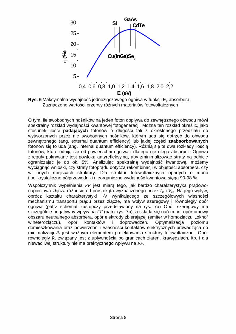
Omówmy pokrótce najważniejsze czynniki, które wpływają na wydajność ogniwa. Wartość prądu zwarcia zależy od tego ile fotonów zostanie zaabsorbowanych w ogniwie, czyli od natężenia światła, a także od wartości ma przerwy energetycznej materiału i jaki jest współczynnik absorpcji. Zauważmy, że im mniejsza jest przerwa energetyczna, tym więcej fotonów ma szansę wytworzyć pary elektron-dziura, więc Isc rośnie, gdy Eg maleje. Z drugiej strony, Voc nie może być wyższe niż bariera na złączu, a więc jego maksymalna wartość jest ograniczona wartością przerwy energetycznej materiału absorbującego światło. Wynika stąd optymalna wartość przerwy energetycznej absorbera równa ok. 1,5 eV. Na rys. 6. przedstawiono teoretycznie obliczoną zależność maksymalnej wydajności ogniwa od przerwy absorbera, otrzymaną przy założeniu, że jedynym źródłem strat jest rekombinacja radiacyjna. W realnym ogniwie o wydajności decyduje na ogół prawdopodobieństwo rekombinacji nieradiacyjnej nośników z udziałem defektów w różnych obszarach ogniwa – w objętości materiału, w obszarach przy-powierzchniowych, także na międzypowierzchni w ogniwach heterozłączowych.
Strona 8
0,4 0,6 0,8 1,0 1,2 1,4 1,6 1,8 2,0 2,2
5
10
15
20
25
30
Cu(InGa)Se2
CdTeGaAs
Si
(%)
(eV)E Rys. 6 Maksymalna wydajność jednozłączowego ogniwa w funkcji Eg absorbera.
Zaznaczono wartości przerwy różnych materiałów fotowoltaicznych
O tym, ile swobodnych nośników na jeden foton dopływa do zewnętrznego obwodu mówi spektralny rozkład wydajności kwantowej fotogeneracji. Można ten rozkład określić, jako stosunek ilości padaj ących fotonów o długości fali z określonego przedziału do wytworzonych przez nie swobodnych nośników, którym uda się dotrzeć do obwodu zewnętrznego (ang. external quantum efficiency) lub jakiej części zaabsorbowanych fotonów się to uda (ang. internal quantum efficiency). Różnią się te dwa rozkłady ilością fotonów, które odbiją się od powierzchni ogniwa i dlatego nie ulega absorpcji. Ogniwo z reguły pokrywane jest powłoką antyrefleksyjną, aby zminimalizować straty na odbicie ograniczając je do ok. 5%. Analizując spektralną wydajność kwantową, możemy wyciągnąć wnioski, czy straty fotoprądu dotyczą rekombinacji w objętości absorbera, czy w innych miejscach struktury. Dla struktur fotowoltaicznych opartych o mono i polikrystaliczne półprzewodniki nieorganiczne wydajność kwantowa sięga 90-98 %.
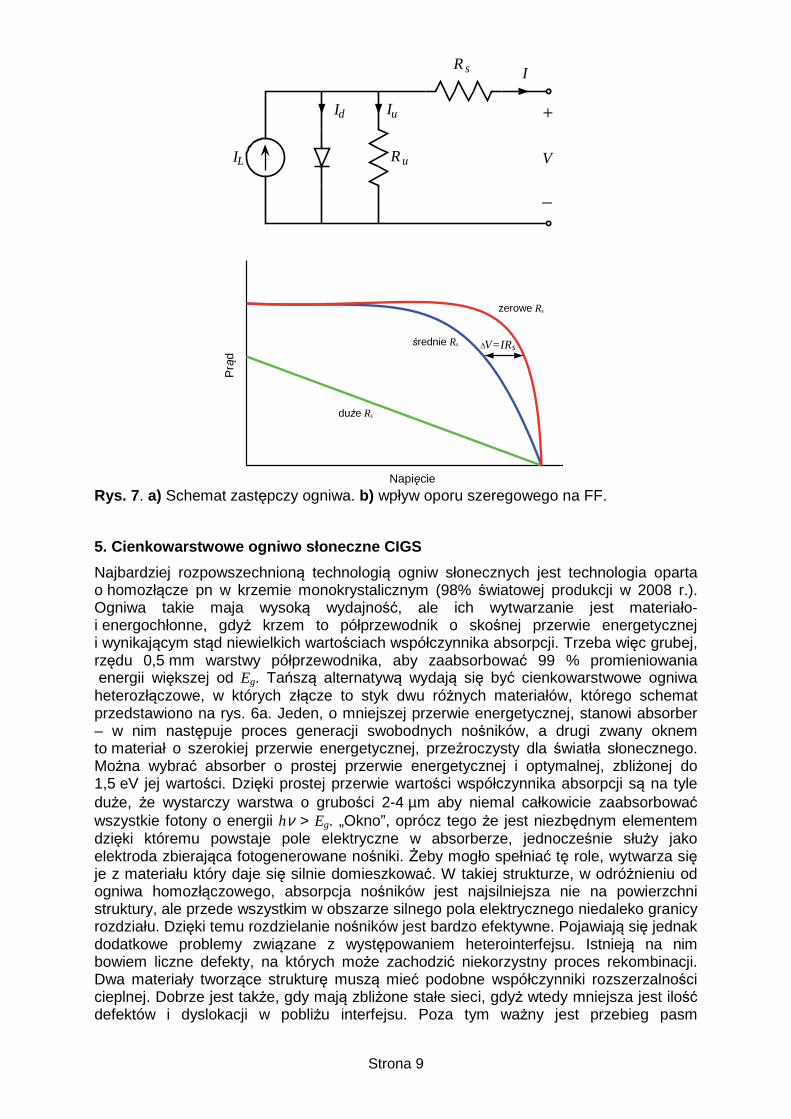
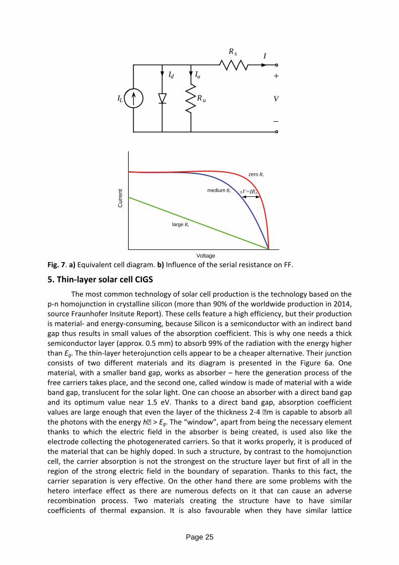
Współczynnik wypełnienia FF jest miarą tego, jak bardzo charakterystyka prądowo- napięciowa złącza różni się od prostokąta wyznaczonego przez Isc i Voc. Na jego wpływ, oprócz kształtu charakterystyki I-V wynikającego ze szczegółowych własności mechanizmu transportu prądu przez złącze, ma wpływ szeregowy i równoległy opór ogniwa (patrz schemat zastępczy przedstawiony na rys. 7a) Opór szeregowy ma szczególnie negatywny wpływ na FF (patrz rys. 7b), a składa się nań m. in. opór omowy obszaru neutralnego absorbera, opór elektrody zbierającej (emiter w homozłączu, „okno” w heterozłączu), opór kontaktów i doprowadzeń. Optymalizacja poziomu domieszkowania oraz powierzchni i własności kontaktów elektrycznych prowadząca do minimalizacji Rs jest ważnym elementem projektowania struktury fotowoltaicznej. Opór równoległy Ru związany jest z upływnością po granicach ziaren, krawędziach, itp. i dla niewadliwej struktury nie ma praktycznego wpływu na FF.
Strona 9
+
V
–
IL
Id Iu
Ru
Rs I
P
rąd
Napięcie
duże Rs
średnie Rs
zerowe Rs
V=IRs
Rys. 7 . a) Schemat zastępczy ogniwa. b) wpływ oporu szeregowego na FF.
5. Cienkowarstwowe ogniwo słoneczne CIGS
Najbardziej rozpowszechnioną technologią ogniw słonecznych jest technologia oparta o homozłącze pn w krzemie monokrystalicznym (98% światowej produkcji w 2008 r.). Ogniwa takie maja wysoką wydajność, ale ich wytwarzanie jest materiało- i energochłonne, gdyż krzem to półprzewodnik o skośnej przerwie energetycznej i wynikającym stąd niewielkich wartościach współczynnika absorpcji. Trzeba więc grubej, rzędu 0,5 mm warstwy półprzewodnika, aby zaabsorbować 99 % promieniowania energii większej od Eg. Tańszą alternatywą wydają się być cienkowarstwowe ogniwa heterozłączowe, w których złącze to styk dwu różnych materiałów, którego schemat przedstawiono na rys. 6a. Jeden, o mniejszej przerwie energetycznej, stanowi absorber – w nim następuje proces generacji swobodnych nośników, a drugi zwany oknem to materiał o szerokiej przerwie energetycznej, przeźroczysty dla światła słonecznego. Można wybrać absorber o prostej przerwie energetycznej i optymalnej, zbliżonej do 1,5 eV jej wartości. Dzięki prostej przerwie wartości współczynnika absorpcji są na tyle duże, że wystarczy warstwa o grubości 2-4 µm aby niemal całkowicie zaabsorbować wszystkie fotony o energii hν > Eg. „Okno”, oprócz tego że jest niezbędnym elementem dzięki któremu powstaje pole elektryczne w absorberze, jednocześnie służy jako elektroda zbierająca fotogenerowane nośniki. Żeby mogło spełniać tę role, wytwarza się je z materiału który daje się silnie domieszkować. W takiej strukturze, w odróżnieniu od ogniwa homozłączowego, absorpcja nośników jest najsilniejsza nie na powierzchni struktury, ale przede wszystkim w obszarze silnego pola elektrycznego niedaleko granicy rozdziału. Dzięki temu rozdzielanie nośników jest bardzo efektywne. Pojawiają się jednak dodatkowe problemy związane z występowaniem heterointerfejsu. Istnieją na nim bowiem liczne defekty, na których może zachodzić niekorzystny proces rekombinacji. Dwa materiały tworzące strukturę muszą mieć podobne współczynniki rozszerzalności cieplnej. Dobrze jest także, gdy mają zbliżone stałe sieci, gdyż wtedy mniejsza jest ilość defektów i dyslokacji w pobliżu interfejsu. Poza tym ważny jest przebieg pasm
Strona 10
przewodnictwa na granicy rozdziału, tzn. brak lub niewielka wartość nieciągłości tych pasm.
oknoabsorber
Eg2
Eg1p
n Rys. 8 a) Heterozłączowe ogniwo słoneczne.
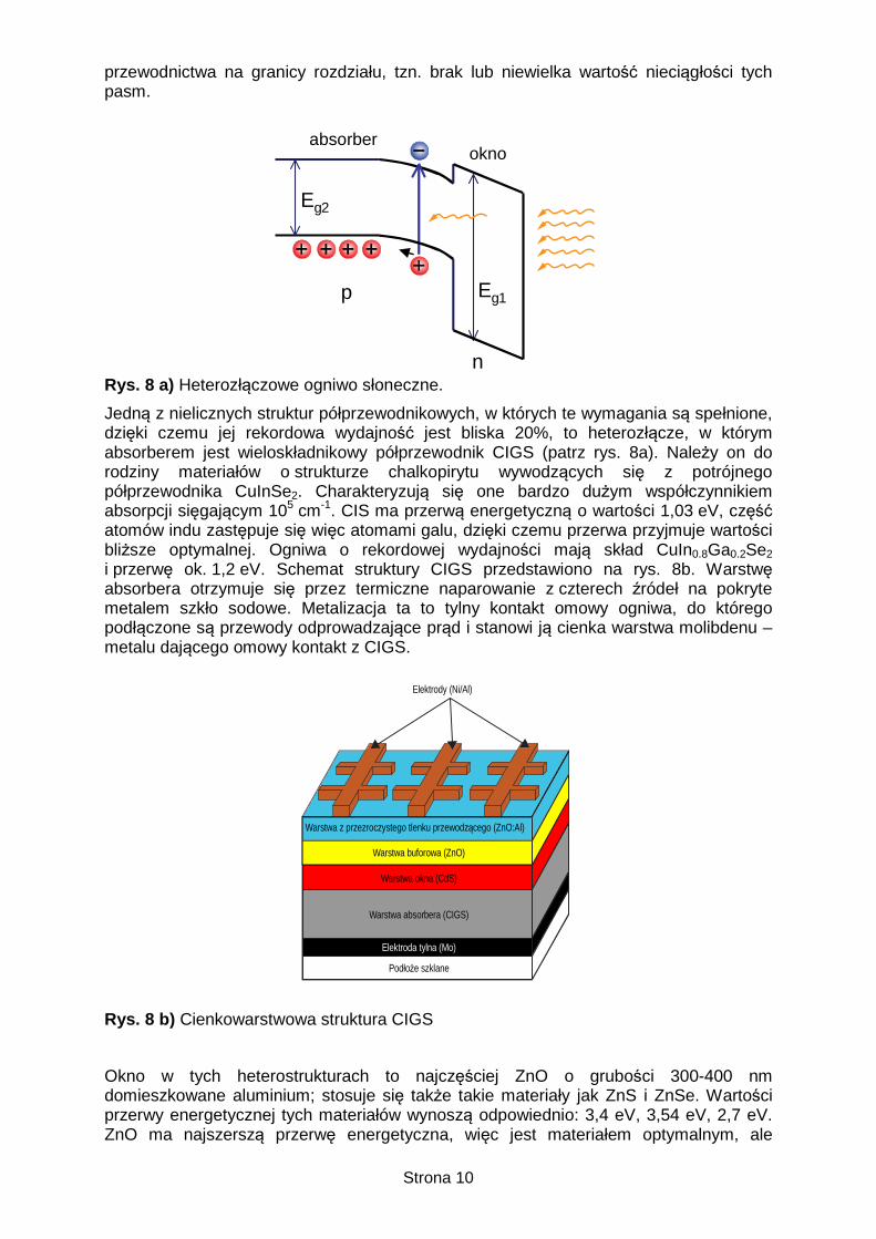
Jedną z nielicznych struktur półprzewodnikowych, w których te wymagania są spełnione, dzięki czemu jej rekordowa wydajność jest bliska 20%, to heterozłącze, w którym absorberem jest wieloskładnikowy półprzewodnik CIGS (patrz rys. 8a). Należy on do rodziny materiałów o strukturze chalkopirytu wywodzących się z potrójnego półprzewodnika CuInSe2. Charakteryzują się one bardzo dużym współczynnikiem absorpcji sięgającym 105 cm-1. CIS ma przerwą energetyczną o wartości 1,03 eV, część atomów indu zastępuje się więc atomami galu, dzięki czemu przerwa przyjmuje wartości bliższe optymalnej. Ogniwa o rekordowej wydajności mają skład CuIn0.8Ga0.2Se2 i przerwę ok. 1,2 eV. Schemat struktury CIGS przedstawiono na rys. 8b. Warstwę absorbera otrzymuje się przez termiczne naparowanie z czterech źródeł na pokryte metalem szkło sodowe. Metalizacja ta to tylny kontakt omowy ogniwa, do którego podłączone są przewody odprowadzające prąd i stanowi ją cienka warstwa molibdenu – metalu dającego omowy kontakt z CIGS.
Podłoże szklane
Elektroda tylna (Mo)
Warstwa absorbera (CIGS)
Warstwa okna (CdS)
Warstwa buforowa (ZnO)
Warstwa z przezroczystego tlenku przewodzącego (ZnO:Al)
Elektrody (Ni/Al)
Rys. 8 b) Cienkowarstwowa struktura CIGS
Okno w tych heterostrukturach to najczęściej ZnO o grubości 300-400 nm domieszkowane aluminium; stosuje się także takie materiały jak ZnS i ZnSe. Wartości przerwy energetycznej tych materiałów wynoszą odpowiednio: 3,4 eV, 3,54 eV, 2,7 eV. ZnO ma najszerszą przerwę energetyczna, więc jest materiałem optymalnym, ale

Strona 11
wysoką wydajność ogniwa uzyskuje się tylko wtedy, gdy pomiędzy ZnO, a absorberem znajduje się warstwa buforowa. Najlepsze rezultaty uzyskuje się, gdy warstwa ta to 40-50 nm siarczku kadmu typu n nanoszonego elektrochemicznie z roztworu. Dobroczynne działanie warstwy buforowej wiąże się prawdopodobnie z lepszym dopasowaniem krawędzi przewodnictwa na interfejsie CdS/CIGS a także z elektrochemicznym oddziaływaniem roztworu używanego w procesie nanoszenia na koncentrację i rodzaj defektów na heterointerfejsie.
Na górnej powierzchni ogniwa napyla się tzw. grid (siatkę) ze stopu niklu z aluminium w postaci cienkich „palców” odchodzących od nieco grubszych „szyn”. Polepsza to zbieranie fotoprądu i redukuje opór szeregowy ogniwa. Cała struktura ma grubość ok. 3 µm i można ją stosunkowo łatwo wytwarzać w skali przemysłowej. W 2009 roku istniało na świecie już kilka zakładów produkujących tego typu ogniwa na świecie, m.in. Heliovolt (USA), Global Solar Energy (USA i Niemcy), Jenn Feng (Tajwan), Wuerth Solar (Niemcy), Shova Shell (Japan), Q-cell&Solibro (Szwecja i Niemcy). Trwają prace nad wdrażaniem technologii CIGS na elastycznych podłożach, m.in. na plastikowych foliach. Jest to kolejny krok mający na celu dalszą redukcję kosztów oraz rozszerzający wachlarz możliwości zastosowań tego typu ogniw słonecznych.
Pytania kontrolne
1. Omów, na czym polega efekt fotowoltaiczny.
2. Narysuj i omów układ zast ępczy ogniwa słonecznego i napis równanie diody.
3. Jaki wpływ na wydajno ść ogniwa ma opór szeregowy?
4. Narysuj charakterystyk ę ciemn ą i charakterystyk ę jasn ą ogniwa słonecznego.
5. Wymień podstawowe parametry charakteryzuj ące wydajno ść ogniwa słonecznego.
6. Co to jest współczynnik wypełnienia?
7. Co to jest wydajno ść kwantowa ogniwa?
Strona 12
6. Wykonanie ćwiczenia Uwaga: Przed przyst ąpieniem do wykonywania ćwiczenia nale ży zapozna ć się z opisem stanowiska i oprogramowania – patrz Dodatki 1, 2 i 3.
Badane ogniwo słoneczne o powierzchni ok. 0,5 cm2 jest zamontowane na podłożu o temperaturze regulowanej w zakresie 0 - 90ºC. Oświetlenie ogniwa stanowi biała dioda LED, której moc można regulować za pomocą potencjometru. Maksymalna moc światła odpowiada w przybliżeniu 1000 W/m2. Do tylnego i przedniego kontaktu dotykają elektrody łączące ogniwo z zewnętrznym obwodem w postaci „czarnej skrzynki” sterowanej komputerowo, która wytwarza żądane napięcia w zakresie od –1 V do +1 V i jednocześnie mierzy prąd płynący przez ogniwo.
1. Wykonać pomiary charakterystyk prądowo-napięciowych ogniwa przy maksymalnym natężeniu zasilającego diodę LED w temperaturach od 5 do 85ºC ze skokiem 10ºC.
2. Wyznaczyć parametry Voc, Isc, FF i η dla wszystkich charakterystyk. Zaobserwować, jak zmieniają się w funkcji temperatury, wykonać ich wykresy i wyciągnąć wnioski.
3. Dla 25ºC wykonać serię charakterystyk dla różnych natężeń światła, zmieniając je tak, aby prąd zwarcia zmniejszał się stopniowo o mniej więcej czynnik 2 oraz zmierzyć charakterystykę ciemną
4. Obliczyć wydajność ogniwa dla różnych natężeń światła, zakładając proporcjonalność między Isc a natężeniem światła. Wyciągnąć wnioski dotyczące działania ogniwa przy słabszym oświetleniu.
5. Porównać ciemną charakterystykę z jasnymi i wyciągnąć wnioski dotyczące „zasady superpozycji” dla badanego ogniwa.
Układ pomiarowy zawierający monochromator wykorzystamy do zmierzenia rozkładu spektralnego wydajności kwantowej. Posłużymy się wyznaczonym uprzednio rozkładem spektralnym widma światła emitowanego przez lampę halogenową użytą w doświadczeniu.
1. Zmierzyć fotoprąd wytwarzany w ogniwie w funkcji długości fali w zakresie 400-1200 nm. Wartości długości fali dobrać tak, aby punkty pomiarowe były równomiernie i wystarczająco gęsto (nie rzadziej niż co 0,05 eV) rozłożone w skali energii.
2. Wykorzystując plik proton flux zawierający rozkład spektralny światła padającego na próbkę, wykonać wykres rozkładu fotoprądu w funkcji energii padających fotonów znormalizowany na jeden padający foton (ponieważ nie znamy dokładnej liczby fotonów padających na strukturę, możemy jedynie określić ten rozkład w jednostkach dowolnych)
3. Wyznaczyć wartość przerwy energetycznej absorbera posługując się metodą „w połowie krawędzi”.
4. Wyznaczyć energię odpowiadającą wysokoenergetycznej krawędzi rozkładu. Czemu on odpowiada?
5. Porównać wartość Voc(T) dla T->0 z wartością przerwy energetycznej otrzymaną z ekstrapolacji zależności Voc(T) do 0oK, wyciągnąć wnioski.
Strona 13
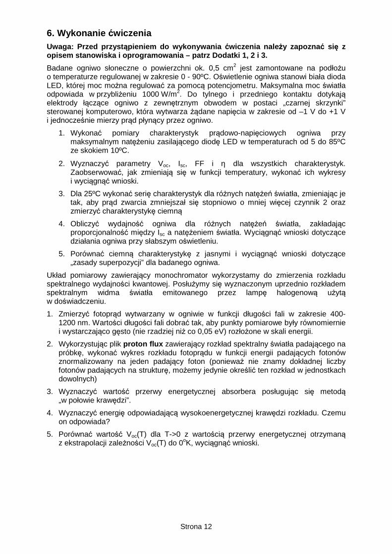
Dodatek 1. Opis stanowiska do pomiaru charakterysty k I-V Do rejestracji charakterystyk IV służy stanowisko przedstawione na zdjęciu poniżej.
Poszczególne elementy zestawu to:
� Zasilacz sterujący mocą diody oświetlającej próbkę
� Włącznik � Regulator natężenia prądu – zakres
regulacji od 0 do 999 mA � Wyświetlacz bieżącej wartości
natężenia prądu (w mA)
� Regulator temperatury próbki
� Włącznik � Regulator temperatury – zakres
regulacji od 0 do 90ºC – regulacji dokonywać, gdy przełącznik � znajduje się w położeniu „ST”
� Przełącznik trybu pracy wyświetlacza: ST: wskazanie ustawionej temperatury MT: bieżący pomiar temperatury
� Wyświetlacz
� Charakterograf I-V
� Moduł do instalacji próbek (widok z góry po otwarciu pokrywy)
� Próbka, widok w powiększeniu:
� Ogniwo Peltier � Elektrody
Komputer z programem zbierającym dane pomiarowe
Patrz opis obsługi programu na stronie następnej.
Przed przyst ąpieniem do pomiarów nale ży upewni ć się, że w module pomiarowym � znajduje si ę próbka, a nast ępnie wł ączyć zasilanie poszczególnych elementów �, � i �.
Strona 14
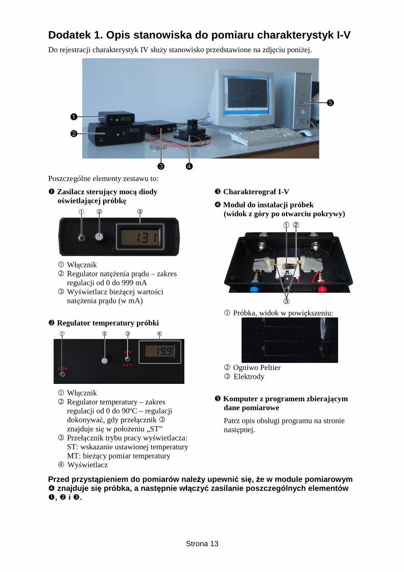
Dodatek 2. Opis stanowiska do pomiaru fotopr ądu Do pomiarów fotoprądu służy stanowisko przedstawione na zdjęciu poniżej.
Poszczególne elementy zestawu to:
� Monochromator
Monochromator – jest przyrządem optycznym umożliwiającym rozszczepienie światła białego i uzyskanie z niego wiązki o węższym spektrum niż wiązka wejściowa.
� Źródło światła � Pokrętło regulacji długości fali � Włącznik � Skala Wylot wiązki o zawężonym widmie
(monochromatycznej)
� Multimetr cyfrowy – w wykorzysty-wanym zestawie umożliwia wyznaczenie natężenia prądu uzyskiwanego z badanej próbki. Miernik pracuje w trybie pomiaru napięcia i jest podłączony równolegle do konwertera prąd-napięcie o współczynniku przetwarzania 105 [V/A].
Page 15
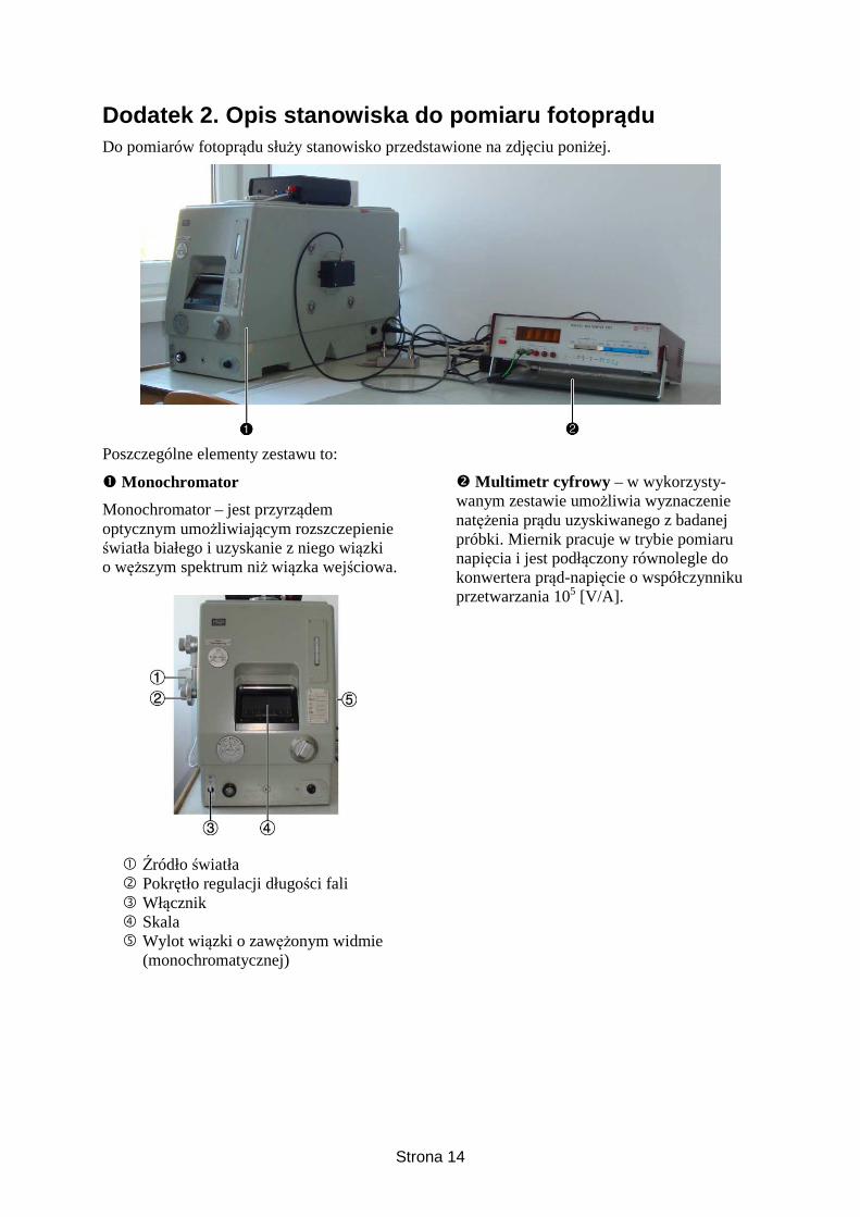
Dodatek 3. Opis programu pomiarowego 1. Kliknij ikon ę IV.exe na pulpicie.
• Na ekranie pojawi się następujące okno:
2. Z menu wybierz polecenie Parametry, żeby ustawi ć warunki pomiaru.
• Na ekranie pojawi się następujące okno:
• Upewnij się, że wprowadzone są właściwe zakresy pomiarów. Uwaga: Nie wolno ustawiać natężeń prądów poza zakresem ± 30 mA.
• Wartości natężenia prądu zasilającego diodę oświetlającą próbkę i temperatury ustawia się przy pomocy odpowiednich pokręteł na zasilaczu diody i zasilaczu ogniwa Peltier – patrz opis stanowiska w Dodatku 1.
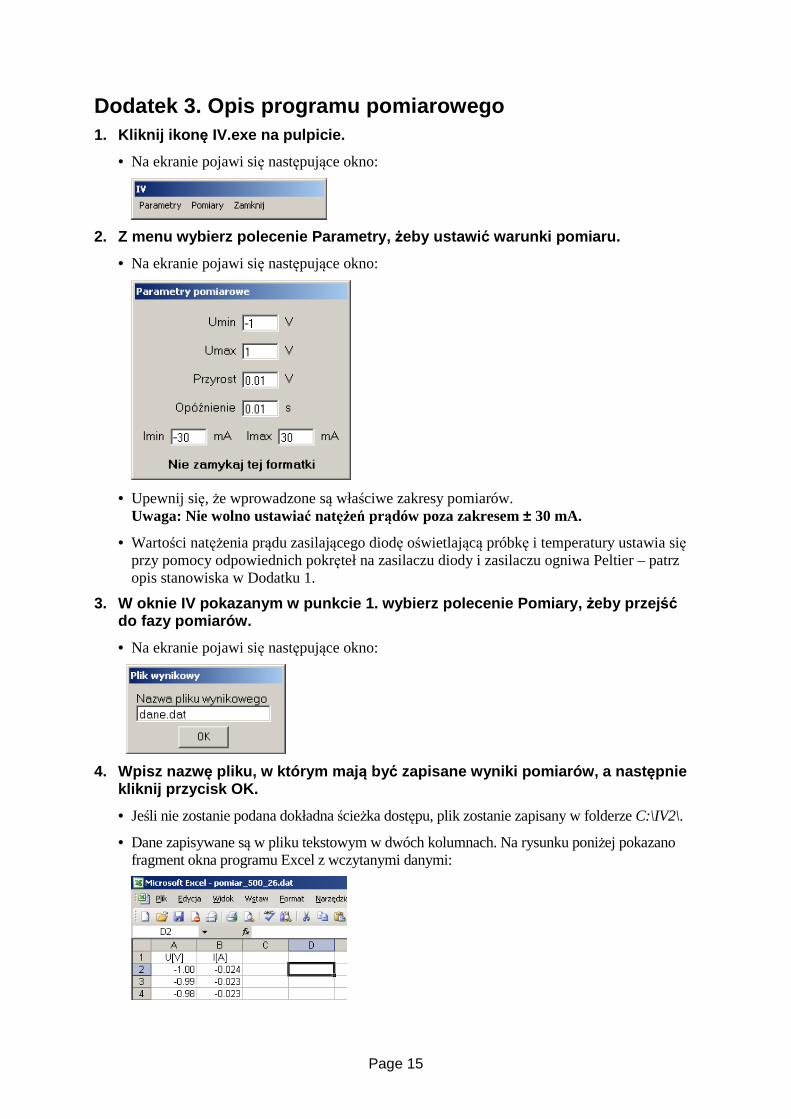
3. W oknie IV pokazanym w punkcie 1. wybierz polece nie Pomiary, żeby przej ść do fazy pomiarów.
• Na ekranie pojawi się następujące okno:
4. Wpisz nazw ę pliku, w którym maj ą być zapisane wyniki pomiarów, a nast ępnie kliknij przycisk OK.
• Jeśli nie zostanie podana dokładna ścieżka dostępu, plik zostanie zapisany w folderze C:\IV2\.
• Dane zapisywane są w pliku tekstowym w dwóch kolumnach. Na rysunku poniżej pokazano fragment okna programu Excel z wczytanymi danymi:
Page 16
• Jeśli nazwa pliku nie zostanie podana, dane pomiarowe nie zostaną zapisane.
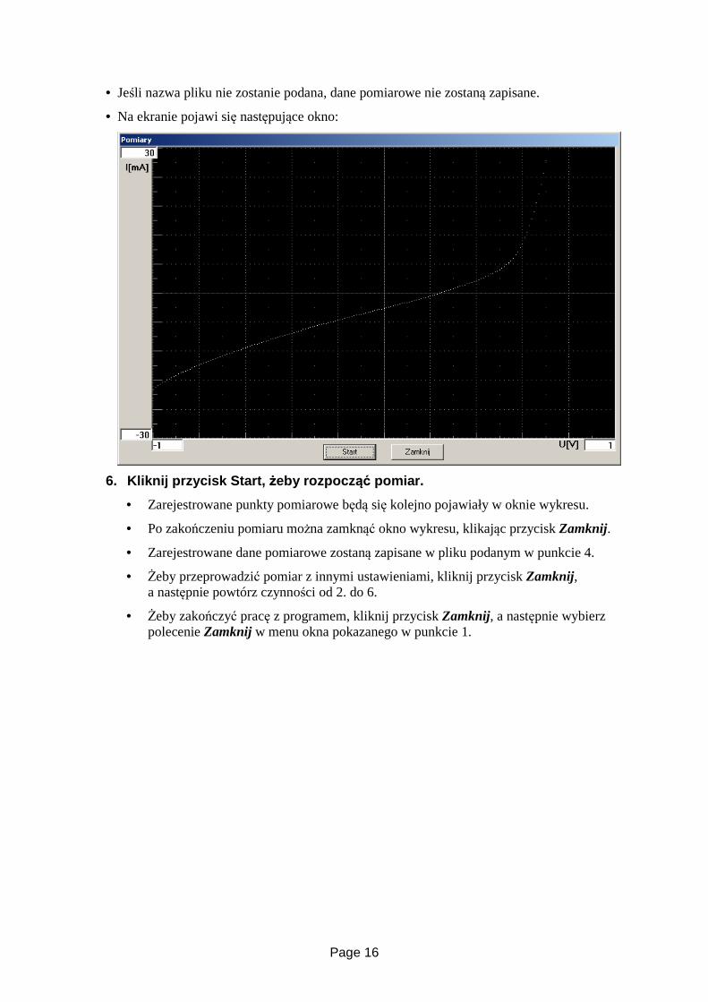
• Na ekranie pojawi się następujące okno:
6. Kliknij przycisk Start, żeby rozpocz ąć pomiar.
• Zarejestrowane punkty pomiarowe będą się kolejno pojawiały w oknie wykresu.
• Po zakończeniu pomiaru można zamknąć okno wykresu, klikając przycisk Zamknij.
• Zarejestrowane dane pomiarowe zostaną zapisane w pliku podanym w punkcie 4.
• Żeby przeprowadzić pomiar z innymi ustawieniami, kliknij przycisk Zamknij, a następnie powtórz czynności od 2. do 6.
• Żeby zakończyć pracę z programem, kliknij przycisk Zamknij, a następnie wybierz polecenie Zamknij w menu okna pokazanego w punkcie 1.
Page 17
Warsaw University of Technology Faculty of Physics Physics II Laboratory - Southern Campus Małgorzata Igalson, Jan Ulaczyk
Excercise no 9
Thin-layer Photovoltaic Cell
1. Solar radiation
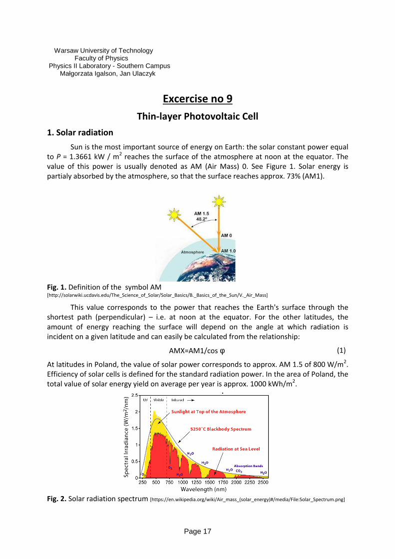
Sun is the most important source of energy on Earth: the solar constant power equal
to P = 1.3661 kW / m2 reaches the surface of the atmosphere at noon at the equator. The
value of this power is usually denoted as AM (Air Mass) 0. See Figure 1. Solar energy is
partialy absorbed by the atmosphere, so that the surface reaches approx. 73% (AM1).
Fig. 1. Definition of the symbol AM [http://solarwiki.ucdavis.edu/The_Science_of_Solar/Solar_Basics/B._Basics_of_the_Sun/V._Air_Mass]
This value corresponds to the power that reaches the Earth's surface through the
shortest path (perpendicular) – i.e. at noon at the equator. For the other latitudes, the
amount of energy reaching the surface will depend on the angle at which radiation is
incident on a given latitude and can easily be calculated from the relationship:
AMX=AM1/cos φ (1)
At latitudes in Poland, the value of solar power corresponds to approx. AM 1.5 of 800 W/m2.
Efficiency of solar cells is defined for the standard radiation power. In the area of Poland, the
total value of solar energy yield on average per year is approx. 1000 kWh/m2.
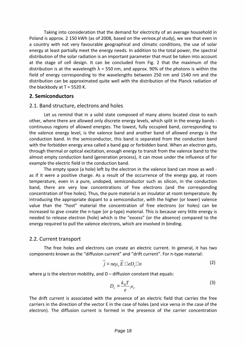
Fig. 2. Solar radiation spectrum [https://en.wikipedia.org/wiki/Air_mass_(solar_energy)#/media/File:Solar_Spectrum.png]
Page 18
Taking into consideration that the demand for electricity of an average household in
Poland is approx. 2 150 kWh (as of 2008, based on the verivox.pl study), we see that even in
a country with not very favourable geographical and climatic conditions, the use of solar
energy at least partially meet the energy needs. In addition to the total power, the spectral
distribution of the solar radiation is an important parameter that must be taken into account
at the stage of cell design. It can be concluded from Fig. 2 that the maximum of the
distribution is at the wavelength λ = 550 nm, and approx. 90% of the photons is within the
field of energy corresponding to the wavelengths between 250 nm and 1540 nm and the
distribution can be approximated quite well with the distribution of the Planck radiation of
the blackbody at T = 5520 K.
2. Semiconductors
2.1. Band structure, electrons and holes
Let us remind that in a solid state composed of many atoms located close to each
other, where there are allowed only discrete energy levels, which split in the energy bands -
continuous regions of allowed energies. The lowest, fully occupied band, corresponding to
the valence energy level, is the valence band and another band of allowed energy is the
conduction band. In the semiconductor, this band is separated from the conduction band
with the forbidden energy area called a band gap or forbidden band. When an electron gets,
through thermal or optical excitation, enough energy to transit from the valence band to the
almost empty conduction band (generation process), it can move under the influence of for
example the electric field in the conduction band.
The empty space (a hole) left by the electron in the valence band can move as well -
as if it were a positive charge. As a result of the occurrence of the energy gap, at room
temperature, even in a pure, undoped, semiconductor such as silicon, in the conduction
band, there are very low concentrations of free electrons (and the corresponding
concentration of free holes). Thus, the pure material is an insulator at room temperature. By
introducing the appropriate dopant to a semiconductor, with the higher (or lower) valence
value than the “host” material the concentration of free electrons (or holes) can be
increased to give create the n-type (or p-type) material. This is because very little energy is
needed to release electron (hole) which is the "excess" (or the absence) compared to the
energy required to pull the valence electrons, which are involved in binding.
2.2. Current transport
The free holes and electrons can create an electric current. In general, it has two
components known as the “diffusion current” and “drift current”. For n-type material:
neDEneµj ee ∇+= (2)
where µ is the electron mobility, and D – diffusion constant that equals:
e
Be µ
e
TkD =
(3)
The drift current is associated with the presence of an electric field that carries the free
carriers in the direction of the vector E in the case of holes (and vice versa in the case of the
electron). The diffusion current is formed in the presence of the carrier concentration
Page 19
gradient and flows to achieve a homogenous distribution of carriers in a volume of
semiconductor. The mobility is defined as the drift velocity per unit of the electric field:
µ=vd/E (4)
and it is a measure of the movement of free carriers in the direction of the field: the more
imperfections (defects, crystal lattice vibration) there are, the smaller it is.
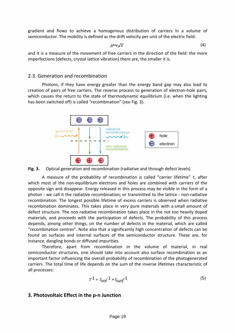
2.3. Generation and recombination
Photons, if they have energy greater than the energy band gap may also lead to
creation of pairs of free carriers. The reverse process to generation of electron-hole pairs,
which causes the return to the state of thermodynamic equilibrium (i.e. when the lighting
has been switched off) is called “recombination” (see Fig. 3).
generationradiativerecombination
non-radiativerecombination
electron
hole
Fig. 3. Optical generation and recombination (radiative and through defect levels)
A measure of the probability of recombination is called “carrier lifetime” τ, after
which most of the non-equilibrium electrons and holes are combined with carriers of the
opposite sign and disappear. Energy released in this process may be visible in the form of a
photon - we call it the radiative recombination; or transmitted to the lattice - non-radiative
recombination. The longest possible lifetime of excess carriers is observed when radiative
recombination dominates. This takes place in very pure materials with a small amount of
defect structure. The non-radiative recombination takes place in the not too heavily doped
materials, and proceeds with the participation of defects. The probability of this process
depends, among other things, on the number of defects in the material, which are called
“recombination centres”. Note also that a significantly high concentration of defects can be
found on surfaces and internal surfaces of the semiconductor structure. These are, for
instance, dangling bonds or diffused impurities.
Therefore, apart from recombination in the volume of material, in real
semiconductor structures, one should take into account also surface recombination as an
important factor influencing the overall probability of recombination of the photogenerated
carriers. The total time of life depends on the sum of the inverse lifetimes characteristic of
all processes:
τ-1 = τvol-1 +τsurf
-1 (5)
3. Photovoltaic Effect in the p-n Junction
Page 20
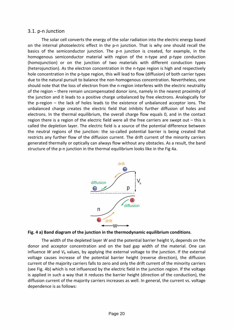
3.1. p-n Junction
The solar cell converts the energy of the solar radiation into the electric energy based
on the internal photoelectric effect in the p-n junction. That is why one should recall the
basics of the semiconductor junction. The p-n junction is created, for example, in the
homogenous semiconductor material with region of the n-type and p-type conduction
(homojunction) or on the junction of two materials with different conduction types
(heterojunction). As the electron concentration in the n-type region is high and respectively
hole concentration in the p-type region, this will lead to flow (diffusion) of both carrier types
due to the natural pursuit to balance the non-homogenous concentration. Nevertheless, one
should note that the loss of electron from the n-region interferes with the electric neutrality
of the region – there remain uncompensated donor ions, namely in the nearest proximity of
the junction and it leads to a positive charge unbalanced by free electrons. Analogically for
the p-region – the lack of holes leads to the existence of unbalanced acceptor ions. The
unbalanced charge creates the electric field that inhibits further diffusion of holes and
electrons. In the thermal equilibrium, the overall charge flow equals 0, and in the contact
region there is a region of the electric field were all the free carriers are swept out – this is
called the depletion layer. The electric field is a source of the potential difference between
the neutral regions of the junction: the so-called potential barrier is being created that
restricts any further flow of the diffusion current. The drift current of the minority carriers
generated thermally or optically can always flow without any obstacles. As a result, the band
structure of the p-n junction in the thermal equilibrium looks like in the Fig 4a.
drift
diffusion
drift
diffusion
n
pV
b
W Fig. 4 a) Band diagram of the junction in the thermodynamic equilibrium conditions.
The width of the depleted layer W and the potential barrier height Vb depends on the
donor and acceptor concentration and on the bad gap width of the material. One can
influence W and Vb values, by applying the external voltage to the junction. If the external
voltage causes increase of the potential barrier height (reverse direction), the diffusion
current of the majority carriers falls to zero and only the drift current of the minority carriers
(see Fig. 4b) which is not influenced by the electric field in the junction region. If the voltage
is applied in such a way that it reduces the barrier height (direction of the conduction), the
diffusion current of the majority carriers increases as well. In general, the current vs. voltage
dependence is as follows:
Page 21
)
TAk
eV(JI
Bodark 1exp −
= (6)
−
=Tk
eEJJ
B
aooo exp
(7)
where A (junction ideality factor) and Io (saturation current) factors depend on the
dominating transport mechanism in the junction (see Table 1).
Table 1. Ideality factor and activation energy of the saturation current vs. IV
curve parameters
Transport mechanism A Ea
Diffusion 1 Eg
Recombination within the absorber volume 1<A<2 AEa=Eg
Recombination through the interface states 1<A<2 Ea=Vb
Same as above with tunnelling of these states A>2 Ea<Vb
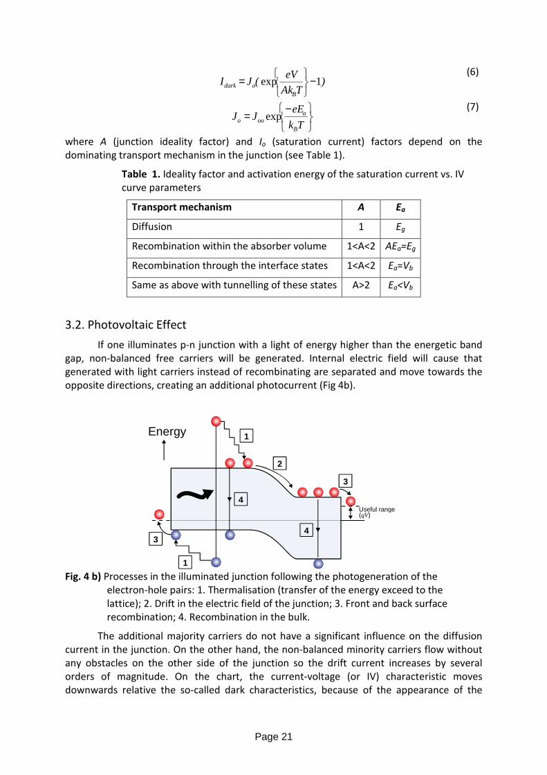
3.2. Photovoltaic Effect
If one illuminates p-n junction with a light of energy higher than the energetic band
gap, non-balanced free carriers will be generated. Internal electric field will cause that
generated with light carriers instead of recombinating are separated and move towards the
opposite directions, creating an additional photocurrent (Fig 4b).
Energy
Useful range(qV)
1
2
3
4
4
1
3
Fig. 4 b) Processes in the illuminated junction following the photogeneration of the
electron-hole pairs: 1. Thermalisation (transfer of the energy exceed to the
lattice); 2. Drift in the electric field of the junction; 3. Front and back surface
recombination; 4. Recombination in the bulk.
The additional majority carriers do not have a significant influence on the diffusion
current in the junction. On the other hand, the non-balanced minority carriers flow without
any obstacles on the other side of the junction so the drift current increases by several
orders of magnitude. On the chart, the current-voltage (or IV) characteristic moves
downwards relative the so-called dark characteristics, because of the appearance of the

Page 22
additional photocurrent with the opposite sign to the diffusion current (Fig. 5). When one
short-cuts the cell, this current (the so-called short circuit current - Isc) will flow in the circuit.
In contrast, when the cell remains open, the charge equivalent to the charge of the minority
charge carriers that will flow on the opposite side of the junction and will recombinate with
the carrier of the opposite sign will cause the potential difference, called open circuit voltage
(Voc).
VoltageC
urre
nt
Lightcharacteristics
Darkcharacteristics
IL
Voc
Vmp
Imp
Isc
Fig. 5 Light and dark IV characteristics of the cell and parameters defining the cell
efficiency
If the illumination produces additional carriers and does not alter the transport
mechanism, the characteristic of the illuminated junction is as follows (superposition rule):
scdl III −= (8)
scB
ol ITAk
eVII −
−
= 1exp (9)
This formula defines the relation between the open circuit voltage and the short circuit
current, because for I=0, V=Voc, and then:
≅
+=
o
scB
o
scBoc I
I
e
TAk
I
I
e
TAkV ln1ln
(10)
One can also notice that if we use the formula (7) for the saturation current, one will obtain
the linear dependence between the open circuit voltage and the temperature (for the fixed
illumination value):
oo
scBa I
ITAkAEeVoc ln|−= (11)
4. Cell Efficiency
The Isc and Voc parameters determine the cell efficiency. If one notices that the
photovoltaic conversion value is defined by the ratio of the maximum produced power to
the power of radiation illuminating the cell:
in
mpmp
P
VI=η
(12)
Usually, the maximum power is expressed through the so-called fill-factor (FF)– see Fig. 5.
Page 23
ocsc
mpmp
VI
VIFF =
(13)
so it can be written as:
in
ocsc
P
FFVI=η (14)
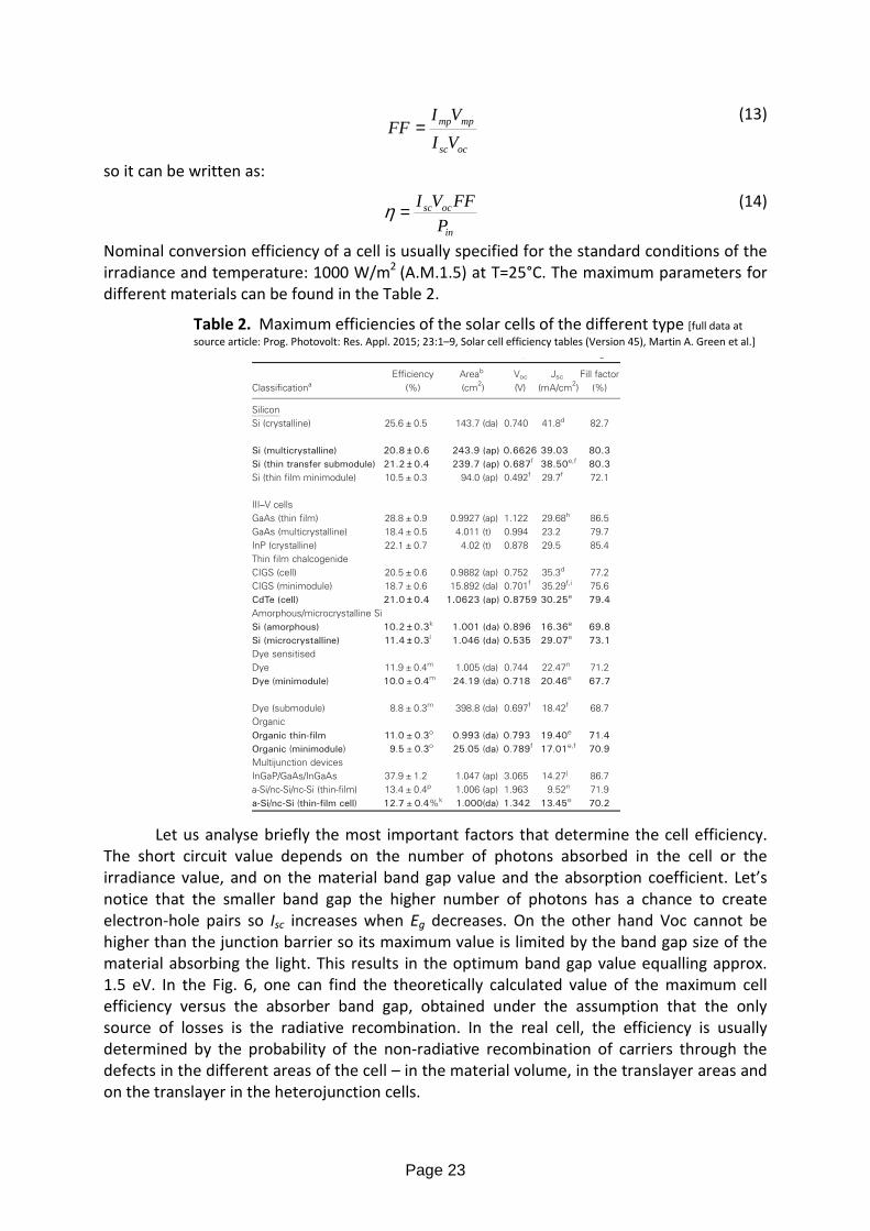
Nominal conversion efficiency of a cell is usually specified for the standard conditions of the
irradiance and temperature: 1000 W/m2
(A.M.1.5) at T=25°C. The maximum parameters for
different materials can be found in the Table 2.
Table 2. Maximum efficiencies of the solar cells of the different type [full data at
source article: Prog. Photovolt: Res. Appl. 2015; 23:1–9, Solar cell efficiency tables (Version 45), Martin A. Green et al.] (IEC 60904-3: 2008, ASTM G-173-03 global).
ClassificationaEfficiency
(%)
Areab
(cm2)
Voc
(V)
Jsc
(mA/cm2)
Fill factor
(%)
Silicon
Si (crystalline) 25.6 ± 0.5 143.7 (da) 0.740 41.8d 82.7
Si (multicrystalline) 20.8 ± 0.6 243.9 (ap) 0.6626 39.03 80.3 FhG-ISE (11/14)
Si (thin transfer submodule) 21.2 ± 0.4 239.7 (ap) 0.687f 38.50e,f 80.3
Si (thin film minimodule) 10.5 ± 0.3 94.0 (ap) 0.492f 29.7f 72.1
III–V cells
GaAs (thin film) 28.8 ± 0.9 0.9927 (ap) 1.122 29.68h 86.5
GaAs (multicrystalline) 18.4 ± 0.5 4.011 (t) 0.994 23.2 79.7 NREL (11/95)
InP (crystalline) 22.1 ± 0.7 4.02 (t) 0.878 29.5 85.4 NREL (4/90)
Thin film chalcogenide
CIGS (cell) 20.5 ± 0.6 0.9882 (ap) 0.752 35.3d 77.2
CIGS (minimodule) 18.7 ± 0.6 15.892 (da) 0.701f 35.29f,i 75.6
CdTe (cell) 21.0 ± 0.4 1.0623 (ap) 0.8759 30.25e 79.4
Amorphous/microcrystalline Si
Si (amorphous) 10.2 ± 0.3k 1.001 (da) 0.896 16.36e 69.8
Si (microcrystalline) 11.4 ± 0.3l 1.046 (da) 0.535 29.07e 73.1
Dye sensitised
Dye 11.9 ± 0.4m 1.005 (da) 0.744 22.47n 71.2
Dye (minimodule) 10.0 ± 0.4m 24.19 (da) 0.718 20.46e 67.7
Dye (submodule) 8.8 ± 0.3m 398.8 (da) 0.697f 18.42f 68.7
Organic
Organic thin-film 11.0 ± 0.3o 0.993 (da) 0.793 19.40e 71.4 AIST
Organic (minimodule) 9.5 ± 0.3o 25.05 (da) 0.789f 17.01e,f 70.9 AIST
Multijunction devices
InGaP/GaAs/InGaAs 37.9 ± 1.2 1.047 (ap) 3.065 14.27j 86.7
a-Si/nc-Si/nc-Si (thin-film) 13.4 ± 0.4p 1.006 (ap) 1.963 9.52n 71.9
a-Si/nc-Si (thin-film cell) 12.7 ± 0.4%k 1.000(da) 1.342 13.45e 70.2 AIST
a
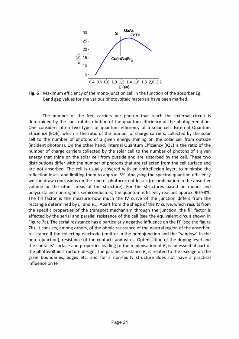
Let us analyse briefly the most important factors that determine the cell efficiency.
The short circuit value depends on the number of photons absorbed in the cell or the
irradiance value, and on the material band gap value and the absorption coefficient. Let’s
notice that the smaller band gap the higher number of photons has a chance to create
electron-hole pairs so Isc increases when Eg decreases. On the other hand Voc cannot be
higher than the junction barrier so its maximum value is limited by the band gap size of the
material absorbing the light. This results in the optimum band gap value equalling approx.
1.5 eV. In the Fig. 6, one can find the theoretically calculated value of the maximum cell
efficiency versus the absorber band gap, obtained under the assumption that the only
source of losses is the radiative recombination. In the real cell, the efficiency is usually
determined by the probability of the non-radiative recombination of carriers through the
defects in the different areas of the cell – in the material volume, in the translayer areas and
on the translayer in the heterojunction cells.
Page 24
0,4 0,6 0,8 1,0 1,2 1,4 1,6 1,8 2,0 2,2
5
10
15
20
25
30
Cu(InGa)Se2
CdTeGaAs
Si
(%)
(eV)E Fig. 6 Maximum efficiency of the mono-junction cell in the function of the absorber Eg.
Band gap values for the various photovoltaic materials have been marked.
The number of the free carriers per photon that reach the external circuit is
determined by the spectral distribution of the quantum efficiency of the photogerenation.
One considers often two types of quantum efficiency of a solar cell: External Quantum
Efficiency (EQE), which is the ratio of the number of charge carriers, collected by the solar
cell to the number of photons of a given energy shining on the solar cell from outside
(incident photons). On the other hand, Internal Quantum Efficiency (IQE) is the ratio of the
number of charge carriers collected by the solar cell to the number of photons of a given
energy that shine on the solar cell from outside and are absorbed by the cell. These two
distributions differ with the number of photons that are reflected from the cell surface and
are not absorbed. The cell is usually covered with an antireflexion layer, to minimise the
reflection loses, and limiting them to approx. 5%. Analysing the spectral quantum efficiency
we can draw conclusions on the kind of photocurrent losses (recombination in the absorber
volume or the other areas of the structure). For the structures based on mono- and
polycristaline non-organic semiconductors, the quantum efficiency reaches approx. 90-98%.
The fill factor is the measure how much the IV curve of the junction differs from the
rectangle determined by Isc and Voc. Apart from the shape of the IV curve, which results from
the specific properties of the transport mechanism through the junction, the fill factor is
affected by the serial and parallel resistance of the cell (see the equivalent circuit shown in
Figure 7a). The serial resistance has a particularly negative influence on the FF (see the figure
7b). It consists, among others, of the ohmic resistance of the neutral region of the absorber,
resistance if the collecting electrode (emitter in the homojunction and the “window” in the
heterojunction), resistance of the contacts and wires. Optimisation of the doping level and
the contacts’ surface and properties leading to the minimisation of Rs is an essential part of
the photovoltaic structure design. The parallel resistance Ru is related to the leakage on the
grain boundaries, edges etc. and for a non-faulty structure does not have a practical
influence on FF.
Page 25
+
V
–
IL
Id Iu
Ru
Rs I
Cur
rent
Voltage
large Rs
medium Rs
zero Rs
Fig. 7. a) Equivalent cell diagram. b) Influence of the serial resistance on FF.
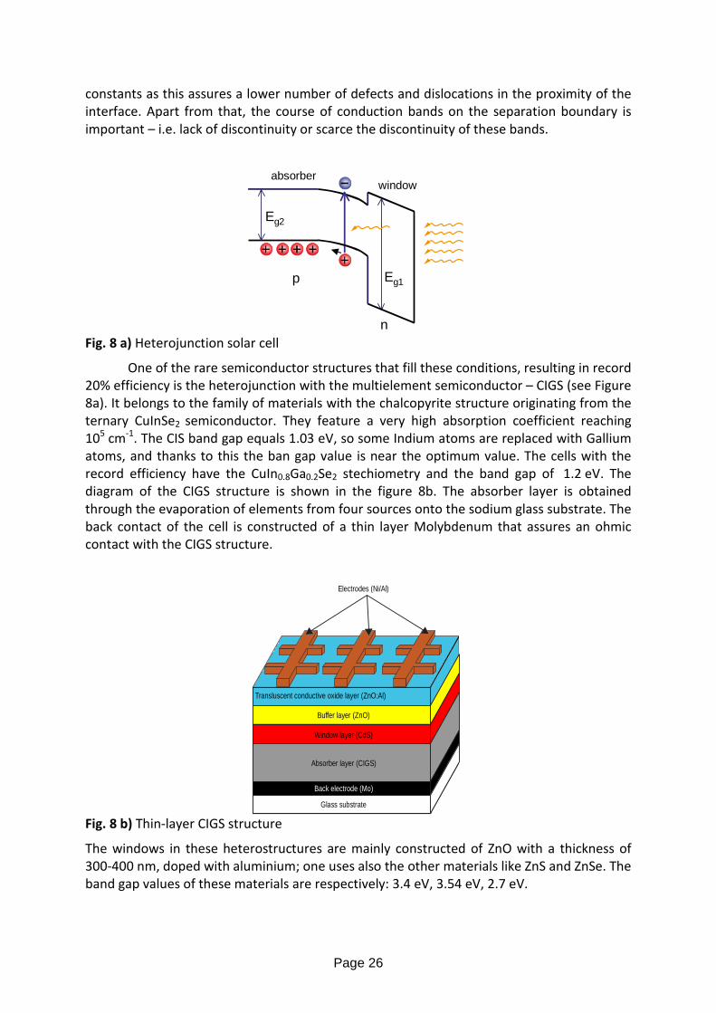
5. Thin-layer solar cell CIGS
The most common technology of solar cell production is the technology based on the
p-n homojunction in crystalline silicon (more than 90% of the worldwide production in 2014,
source Fraunhofer Insitute Report). These cells feature a high efficiency, but their production
is material- and energy-consuming, because Silicon is a semiconductor with an indirect band
gap thus results in small values of the absorption coefficient. This is why one needs a thick
semiconductor layer (approx. 0.5 mm) to absorb 99% of the radiation with the energy higher
than Eg. The thin-layer heterojunction cells appear to be a cheaper alternative. Their junction
consists of two different materials and its diagram is presented in the Figure 6a. One
material, with a smaller band gap, works as absorber – here the generation process of the
free carriers takes place, and the second one, called window is made of material with a wide
band gap, translucent for the solar light. One can choose an absorber with a direct band gap
and its optimum value near 1.5 eV. Thanks to a direct band gap, absorption coefficient
values are large enough that even the layer of the thickness 2-4 m is capable to absorb all
the photons with the energy h > Eg. The “window”, apart from being the necessary element
thanks to which the electric field in the absorber is being created, is used also like the
electrode collecting the photogenerated carriers. So that it works properly, it is produced of
the material that can be highly doped. In such a structure, by contrast to the homojunction
cell, the carrier absorption is not the strongest on the structure layer but first of all in the
region of the strong electric field in the boundary of separation. Thanks to this fact, the
carrier separation is very effective. On the other hand there are some problems with the
hetero interface effect as there are numerous defects on it that can cause an adverse
recombination process. Two materials creating the structure have to have similar
coefficients of thermal expansion. It is also favourable when they have similar lattice
Page 26
constants as this assures a lower number of defects and dislocations in the proximity of the
interface. Apart from that, the course of conduction bands on the separation boundary is
important – i.e. lack of discontinuity or scarce the discontinuity of these bands.
windowabsorber
Eg2
Eg1p
n Fig. 8 a) Heterojunction solar cell
One of the rare semiconductor structures that fill these conditions, resulting in record
20% efficiency is the heterojunction with the multielement semiconductor – CIGS (see Figure
8a). It belongs to the family of materials with the chalcopyrite structure originating from the
ternary CuInSe2 semiconductor. They feature a very high absorption coefficient reaching
105 cm
-1. The CIS band gap equals 1.03 eV, so some Indium atoms are replaced with Gallium
atoms, and thanks to this the ban gap value is near the optimum value. The cells with the
record efficiency have the CuIn0.8Ga0.2Se2 stechiometry and the band gap of 1.2 eV. The
diagram of the CIGS structure is shown in the figure 8b. The absorber layer is obtained
through the evaporation of elements from four sources onto the sodium glass substrate. The
back contact of the cell is constructed of a thin layer Molybdenum that assures an ohmic
contact with the CIGS structure.
Glass substrate
Back electrode (Mo)
Absorber layer (CIGS)
Window layer (CdS)
Buffer layer (ZnO)
Transluscent conductive oxide layer (ZnO:Al)
Electrodes (Ni/Al)
Fig. 8 b) Thin-layer CIGS structure
The windows in these heterostructures are mainly constructed of ZnO with a thickness of
300-400 nm, doped with aluminium; one uses also the other materials like ZnS and ZnSe. The
band gap values of these materials are respectively: 3.4 eV, 3.54 eV, 2.7 eV.

Page 27
ZnO features the largest band gap so it is an optimum material but the highest cell efficiency
is obtained only in case when there is buffer layer between ZnO and the absorber. The best
results are obtained when the buffer layer is made of 40-50 nm of n-type cadmium sulphate
electrochemically deposited from the solution. A beneficial action of the buffer layer is
probably related with the better matching if the conduction edge on the CdS/CIGS and with
the electrochemical impact of the solution used in the process of the deposition on the
concentration and type of defects on the heteroiterface. On the top layer of the cell, a so-
called grid is sprayed. The grid is made of the nickel-aluminium alloy that is formed like
narrow fingers departing from a larger “rails”. This improves collection of the photocurrent
and reduces the serial resistance of the cell. The entire structure is 3 m and can be
relatively easily produced industrially. There are several plants producing these cells
worldwide: Heliovolt (USA), Global Solar Energy (USA and Germany), Jenn Feng (Taiwan),
Wuerth Solar (Germany), Shova Shell (Japan), Q-cell&Solibro (Sweden and Germany). There
are also works on the implementation of the CIGS technology in elastic substrates, for
example plastic foil. This is the next step, leading to the further cost reduction and
expanding the scope of possible applications of the solar cells of that type.
Test questions
1. Explain the nature of the photovoltaic effect.
2. Draw and explain the equivalent diagram of the photovoltaic cell and
write down the diode equation.
3. What is the influence of the serial resistance on the cell efficiency?
4. Draw the dark and light characteristics of a solar cell.
5. Name and describe the most important parameters characterising the
efficiency of the solar cell.
6. What is the fill factor?
7. What is the quantum efficiency of the cell?

Page 28
6. Tasks to be completed
Caution: Before starting the experiments please refer to the Appendix 1, 2 and 3 to learn
more on the measurement setup and the software.
For calculations assume maximum photo flux Fmax=800 W/m2, cell area S =5 mm
2.
Please confirm the above with your tutor.
1. Measure I-V characteristics at room temperature at various light intensities: Φmax,
0.5Φmax, 1/4Φmax, 1/8Φmax, 1/16Φmax, 1/32 Φmax, dark. Calculate a dependence of
efficiency on light intensity. Which parameter is mostly responsible for the changes? Plot
ln(Isc) vs Voc and calculate ideality factor of the diode. Put dark I-V curve on the same plot
and conclude on the superposition principle.
2. Measure I-V characteristics at a maximum light intensity at temperatures between 5 and
60oC with 10
oC step. Plot Voc vs temperature and extrapolate the plot to 0 K. Read the
extrapolated value of Voc and compare to the band gap of material derived from spectral
dependence of short circuit current (task 3). Repeat the measurement at 0.5Φmax and
compare the result.
Calculate a dependence of efficiency on temperature (take data for Φmax) and write
conclusions on the performance of the cell at low and high temperature. Which
parameter is most affected by temperature?
3. Measure spectral distribution of short circuit current (external quantum efficiency). Use
“photon flux” file and normalize the spectrum to the same photon flux at each
wavelength. Make a plot of the normalized Isc vs photon energy and read the value of
band gap energy. Comment on the shape of distribution.
Literature: http://pveducation.org/pvcdrom
Chapter 4 : Solar cell operation
Page 29
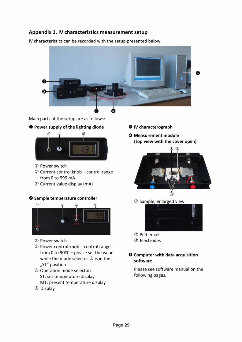
Appendix 1. IV characteristics measurement setup
IV characteristics can be recorded with the setup presented below.
Main parts of the setup are as follows:
� Power supply of the lighting diode
� Power switch
� Current control knob – control range
from 0 to 999 mA
� Current value display (mA)
� Sample temperature controller
� Power switch
� Power control knob – control range
from 0 to 90ºC – please set the value
while the mode selector � is in the
„ST” position
� Operation mode selector:
ST: set temperature display
MT: present temperature display
� Display
� IV characterograph
� Measurement module
(top view with the cover open)
� Sample, enlarged view:
� Peltier cell
� Electrodes
Computer with data acquisition
software
Please see software manual on the
following pages.
Page 30
Before starting the measurement please make sure that the sample is properly positioned
in the measurement module �. Afterwards, please set the power of the other modules
(�, � and �) on.
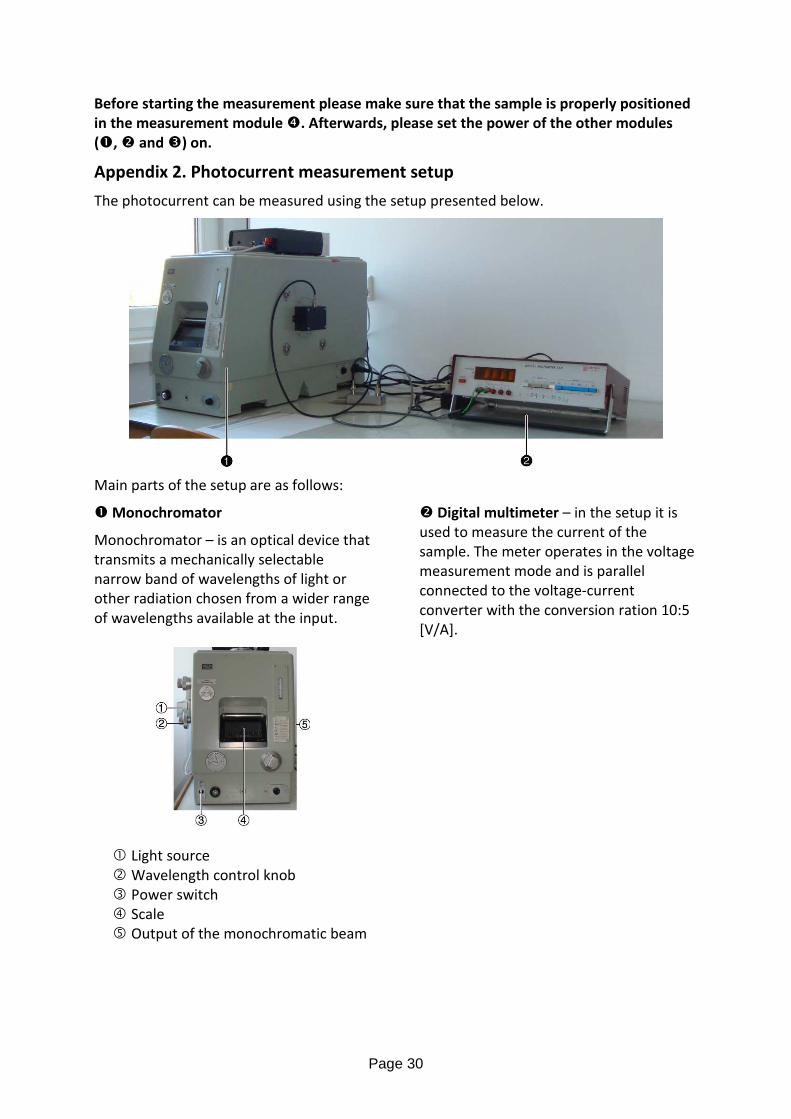
Appendix 2. Photocurrent measurement setup
The photocurrent can be measured using the setup presented below.
Main parts of the setup are as follows:
� Monochromator
Monochromator – is an optical device that
transmits a mechanically selectable
narrow band of wavelengths of light or
other radiation chosen from a wider range
of wavelengths available at the input.
� Light source
� Wavelength control knob
� Power switch
� Scale
Output of the monochromatic beam
� Digital multimeter – in the setup it is
used to measure the current of the
sample. The meter operates in the voltage
measurement mode and is parallel
connected to the voltage-current
converter with the conversion ration 10:5
[V/A].

Strona 31
Appendix 3. Software description
1. Click the IV.exe icon on the desktop.
• A following window will appear on the screen:
2. From the menu bar choose Parametry to set the measurement conditions.
• A following window will appear on the screen:
• Please make sure that the proper measurement ranges are set.
Caution: Do not set the current values out of the range ± 30 mA.
• Value of the current supplying the light diode and the temperature are set with the
knobs on the diode power supply and on the power supply of the Peltier cell – refer
Appendix 1.
3. In the window IV shown in the step 1 choose Pomiary command, to move to the
measurement phase.
• A following window will appear on the screen:
4. Please give a name to the file where the measurement results are to be saved and then
please click OK button.
• If the path is not given, the file will be saved in the C:\IV2\ folder.
• The data is saved in the text file in two columns. The part of the Excel window with the
data is shown in the image below:
• If the file name is not given, the data will not be saved to disk.
Strona 32
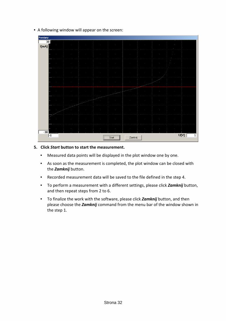
• A following window will appear on the screen:
5. Click Start button to start the measurement.
• Measured data points will be displayed in the plot window one by one.
• As soon as the measurement is completed, the plot window can be closed with
the Zamknij button.
• Recorded measurement data will be saved to the file defined in the step 4.
• To perform a measurement with a different settings, please click Zamknij button,
and then repeat steps from 2 to 6.
• To finalize the work with the software, please click Zamknij button, and then
please choose the Zamknij command from the menu bar of the window shown in
the step 1.