
Artur Jędrusyna, Krzysztof Tomczuk
44
Projekt współfinansowany ze środków Unii Europejskiej w ramach Europejskiego Funduszu Społecznego ROZWÓJ POTENCJAŁU I OFERTY DYDAKTYCZNEJ POLITECHNIKI WROCŁAWSKIEJ Wrocław University of Technology Refrigeration and Cryogenics Artur Jędrusyna, Krzysztof Tomczuk MECHATRONICS AND CONTROL SYSTEMS LABORATORY HANDBOOK Wrocław 2011
Transcript of Artur Jędrusyna, Krzysztof Tomczuk
Projekt współfinansowany ze środków Unii Europejskiej w ramach Europejskiego Funduszu Społecznego
ROZWÓJ POTENCJAŁU I OFERTY DYDAKTYCZNEJ POLITECHNIKI WROCŁAWSKIEJ
Wrocław University of Technology
Refrigeration and Cryogenics
Artur Jędrusyna, Krzysztof Tomczuk
MECHATRONICS
AND CONTROL SYSTEMS
LABORATORY HANDBOOK
Wrocław 2011
Wrocław University of Technology
Refrigeration and Cryogenics
Artur Jędrusyna, Krzysztof Tomczuk
MECHATRONICS
AND CONTROL SYSTEMS LABORATORY HANDBOOK
Compressor Refrigeration Systems, Heat Pumps,
\
Wrocław 2011
Copyright © by Wrocław University of Technology
Wrocław 2011
Reviewer: Tadeusz Mikulczyński
ISBN 978-83-62098-58-3
Published by PRINTPAP Łódź, www.printpap.pl

Contents:
Introduction
The prerequisites
1. Microcontrollers
1.1 Introduction
1.2 Projects
1.2.1 The First Project
1.2.2 The Second Project
1.2.3 The Third Project
1.2.4 The Fourth Project
1.2.5 The Fifth Project
Literature
2.Process automation using PLCs
2.1 Introduction
2.2 Simatic S7-200 PLC
2.3 Didactic Multi-Production System (MPS) based on Festo equipment
2.4 Laboratory tasks
2.4.1 Preliminary tasks
2.4.2 Detailed tasks
Literature
3
Introduction
This book is intended as the basic textbook for students attending Mechatronics and Control System
Lab held at the Faculty of Mechanical and Power Engineering at Wrocław University of
Technology. The main body of the book encompasses two parts – the first is a brief course in
microcontrollers and its applications and the second describes the principal applications of the
programmable logic controllers (PLC) in mechatronics. In both parts of the textbook some
examples of programmes or applications were given, starting from relatively simple tasks to more
complex projects.
The prerequisites
It is assumed that the reader knows basic algebra rules and is familiarized with both electrical
circuits theory and fundamentals of electronic engineering (especially logic circuits theory). Some
experience related to programming would also be an advantage.
4
1. Microcontrollers
1.1. Introduction
A control system could usually be regarded as a “black box” with multiple inputs and outputs,
processing input signals and producing - as a response - output signals. The relation between input
and output signals could be described solely by the hardware configuration of the system
(containing switches, relays, pushbuttons, etc.) – such a case could be described as a system with a
“hardware fixed algorithm”; one should note that every modification of a hardware fixed algorithm
requires a complete rebuilding of the control system configuration. In a more flexible configuration
the control system has the constant structure, but an algorithm of its operation is located in an
external memory (which is often called a program memory). The contents of this memory could be
easily modified without the need for changing the hardware. Such an approach allows an easy
modification of the behaviour of the system without the need for its complete re-construction. The
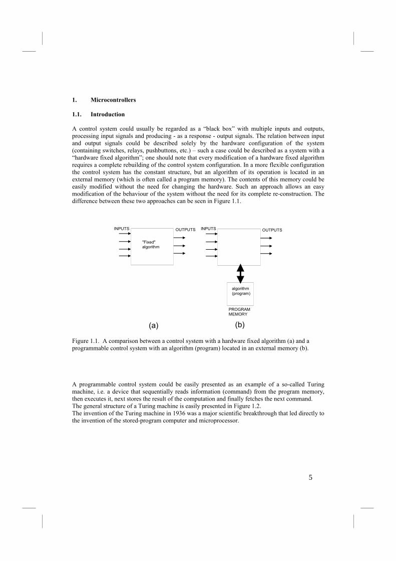
difference between these two approaches can be seen in Figure 1.1.
INPUTS OUTPUTS
"Fixed"algorithm
INPUTS OUTPUTS
algorithm
(program)
PROGRAMMEMORY
(a) (b)
Figure 1.1. A comparison between a control system with a hardware fixed algorithm (a) and a
programmable control system with an algorithm (program) located in an external memory (b).
A programmable control system could be easily presented as an example of a so-called Turing
machine, i.e. a device that sequentially reads information (command) from the program memory,
then executes it, next stores the result of the computation and finally fetches the next command.
The general structure of a Turing machine is easily presented in Figure 1.2.
The invention of the Turing machine in 1936 was a major scientific breakthrough that led directly to
the invention of the stored-program computer and microprocessor.
5

1 10 1 0 1 0 0 1
moving CPU
read / write
device
memory tape
Figure 1.2. The general structure of the Turing machine. CPU= Central Processing Unit.
One of the best examples of a Turing machine could be a microcontroller, which can be treated as a
simple programmable device.
The general structure of a microcontroller (see Figure 1.3) bears a significant resemblance to the
Turing machine. Instead of memory tape the structure uses a program memory containing cells
described by numerical addresses. The commands are cyclically fetched from the non-volatile
program memory (ROM – Read-Only-Memory), then decoded and executed. The decoding takes
place inside the CPU (Central Processing Unit), which can be regarded as the “brain” of the
microprocessor. The results of computations, measurements and other user data are stored in the
volatile memory (RAM – Random Access Memory). The speed of operation is determined by an
external clock signal (usually produced by quartz or RC oscillator). The interface of the processor to
the outside world is possible via bi-directional input/output ports (I/O ports). These ports can be
used for testing signals from switches, sensors, pushbuttons, etc. They can also be a source of
signals switching on lamps, buzzers, displays and other devices.
INPUT/OUTPUT
PORTS
CPU
DATAMEMORY
(RAM)
PROGRAM
MEMORY(ROM)
INTERNAL BUS
EXTERNALSIGNALS
CLOCK
SIGNAL
Figure 1.3. The general structure of a simple microcontroller. Please note the resemblance to the
Turing machine.
6

In classic microprocessors, RAM and ROM memories and I/O ports usually are located in separate
integrated circuits. In order to build a working computer the designer has to use many separate
integrated circuits. However, in microcontrollers all the peripheral devices are located inside the
same integrated circuit – this is the reason for the other name for a microcontroller – a single
board computer.
We should note that a microcontroller (also described as MCU = Microcontroller Unit) usually
performs repeatedly the following consecutive actions:
Command fetching Command decoding Scanning input ports Execution of the command Storing the results Updating output ports Fetching of the next command
An abovementioned sequence of actions is called a machine cycle.
A more detailed description of microcontroller operation is beyond the scope of this textbook;
however, the reader may easily find more information in numerous excellent books on the subject
(see e.g. [1],[2].[3]).
An example of a single microcontroller (Motorola/Freescale 68HC05J1A) is shown in Figure 1.4 -
Please note all the parts mentioned before: data and program memory, CPU and I/O ports.
Figure 1.4. The internal diagram of MC68HC05J1A microcontroller (© Motorola/Freescale).
7
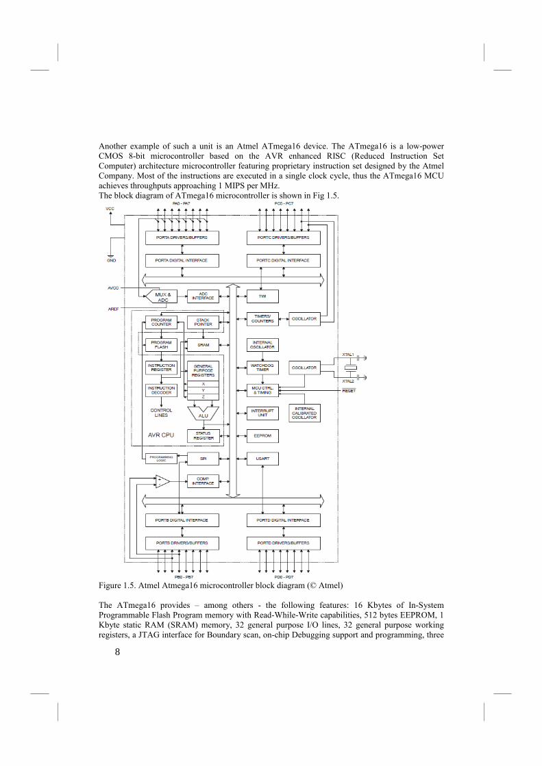
Another example of such a unit is an Atmel ATmega16 device. The ATmega16 is a low-power
CMOS 8-bit microcontroller based on the AVR enhanced RISC (Reduced Instruction Set
Computer) architecture microcontroller featuring proprietary instruction set designed by the Atmel
Company. Most of the instructions are executed in a single clock cycle, thus the ATmega16 MCU
achieves throughputs approaching 1 MIPS per MHz.
The block diagram of ATmega16 microcontroller is shown in Fig 1.5.
Figure 1.5. Atmel Atmega16 microcontroller block diagram (© Atmel)
The ATmega16 provides – among others - the following features: 16 Kbytes of In-System
Programmable Flash Program memory with Read-While-Write capabilities, 512 bytes EEPROM, 1
Kbyte static RAM (SRAM) memory, 32 general purpose I/O lines, 32 general purpose working
registers, a JTAG interface for Boundary scan, on-chip Debugging support and programming, three
8
Timer/Counters with compare modes, Internal and External Interrupts, a universal programmable
serial mode transmitter/receiver (USART), an 8-channel, 10-bit analog-to-digital converter (ADC)
and a programmable Watchdog Timer (a dedicated timer circuit protecting against program hang-up
and erratic operation).
Atmega16 MCU Pin Descriptions
VCC Digital supply voltage.
G3D Ground.
Port A (PA7..PA0) Port A serves as the analog input to the A/D Converter.
Port A also serves as an 8-bit bi-directional I/O port, if the A/D Converter is not used. Port pins
can provide internal pull-up resistors (selected for each bit). The Port A output buffers have
symmetrical drive characteristics with both high sink and source capability. When pins PA0 to PA7
are used as inputs and are externally pulled low, they will source current if the internal pull-up
resistors are activated. The Port A pins are tri-stated when a reset condition becomes active,
even if the clock is not running.
Port B (PB7..PB0) Port B is an 8-bit bi-directional I/O port with internal pull-up resistors
(selected for each bit). The Port B output buffers have symmetrical drive characteristics with both
high sink and source capability. As inputs, Port B pins that are externally pulled low will source
current if the pull-up resistors are activated. The Port B pins are tri-stated when a reset condition
becomes active, even if the clock is not running
Port C (PC7..PC0) Port C is an 8-bit bi-directional I/O port with internal pull-up resistors
(selected for each bit). The Port C output buffers have symmetrical drive characteristics with both
high sink and source capability. As inputs, Port C pins that are externally pulled low will source
current if the pull-up resistors are activated. The Port C pins are tri-stated when a reset condition
becomes active, even if the clock is not running. If the JTAG interface is enabled, the pull-up
resistors on pins PC5(TDI), PC3(TMS) and PC2(TCK) will be activated even if a reset occurs.
Port C also serves the functions of the JTAG interface and other special features of the
ATmega16 processor.
Port D (PD7..PD0) Port D is an 8-bit bi-directional I/O port with internal pull-up resistors
(selected for each bit). The Port D output buffers have symmetrical drive characteristics with both
high sink and source capability. As inputs, Port D pins that are externally pulled low will source
current if the pull-up resistors are activated. The Port D pins are tri-stated when a reset condition
becomes active, even if the clock is not running.
RESET Reset Input. A low level on this pin for longer than the minimum pulse length will
generate a reset, even if the clock is not running.
XTAL1 Input to the inverting Oscillator amplifier and input to the internal clock operating
circuit.
XTAL2 Output from the inverting Oscillator amplifier.
AVCC AVCC is the supply voltage pin for Port A and the A/D Converter. It should be
externally connected to VCC, even if the ADC is not used. If the ADC is used, it should be
connected to VCC through a low-pass filter.
9

AREF AREF is the analog reference pin for the A/D Converter.
Additional information about the ATmega MCU family can be found in datasheets and excellent
application notes published by the producer (please refer to www.atmel.com ).
Gotronik AVR prototyping board
The AVR ATmega v1 prototyping board is an example of a simple development system that can be
used both by students and experienced programmers during programming of Atmel AVR and
ATmega families of 8-bit microcontrollers, especially AT90S8535, ATMEGA8535, ATMEGA16
and ATMEGA32 chips (40 pin DIP case versions). The board includes also a set of the most
popular and useful peripheral devices. All the connections can be made using flexible cables with
snap-on connectors. Moreover, the circuit board encompasses an universal test area with solder
pads located in square 0,1” (2,54 mm) raster. This area can be used for custom circuits built by the
user. The board was designed and is manufactured by the Gotronik Company (Wrocław, Poland).
All the experiments described in this part of this textbook will use Gotronik AVR ATmega v1
prototyping board as the hardware platform.
The circuit board encompasses numerous peripheral devices. The more detailed description can be
found below.
The layout of the front panel of the module is shown in Fig. 1.6:
Figure 1.6. The layout of the ATmega development board by Gotronik Ltd.
10
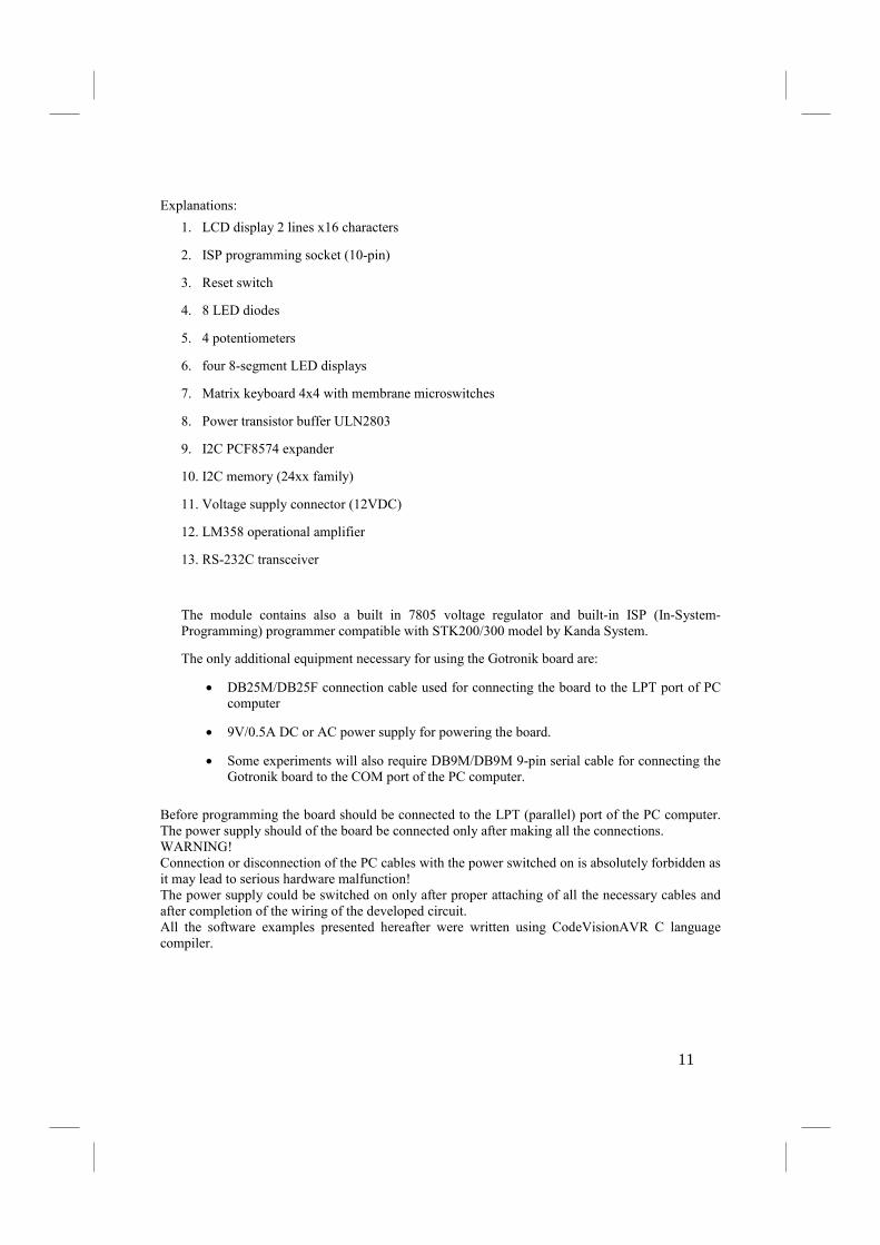
Explanations:
1. LCD display 2 lines x16 characters
2. ISP programming socket (10-pin)
3. Reset switch
4. 8 LED diodes
5. 4 potentiometers
6. four 8-segment LED displays
7. Matrix keyboard 4x4 with membrane microswitches
8. Power transistor buffer ULN2803
9. I2C PCF8574 expander
10. I2C memory (24xx family)
11. Voltage supply connector (12VDC)
12. LM358 operational amplifier
13. RS-232C transceiver
The module contains also a built in 7805 voltage regulator and built-in ISP (In-System-
Programming) programmer compatible with STK200/300 model by Kanda System.
The only additional equipment necessary for using the Gotronik board are:
• DB25M/DB25F connection cable used for connecting the board to the LPT port of PC
computer
• 9V/0.5A DC or AC power supply for powering the board.
• Some experiments will also require DB9M/DB9M 9-pin serial cable for connecting the
Gotronik board to the COM port of the PC computer.
Before programming the board should be connected to the LPT (parallel) port of the PC computer.
The power supply should of the board be connected only after making all the connections.
WARNING!
Connection or disconnection of the PC cables with the power switched on is absolutely forbidden as
it may lead to serious hardware malfunction!
The power supply could be switched on only after proper attaching of all the necessary cables and
after completion of the wiring of the developed circuit.
All the software examples presented hereafter were written using CodeVisionAVR C language
compiler.
11
CodeVision AVR C compiler
CodeVisionAVR is a C cross-compiler, Integrated Development Environment and Automatic
Program Generator designed for the Atmel AVR family of microcontrollers. The tool was
developed by HP InfoTech Company.
The program is a native 32bit application that runs under the Windows 95, 98, NT 4, 2000 and XP
operating systems. The C cross-compiler implements nearly all the elements of the ANSI C
language, as allowed by the AVR architecture, with some features added to take advantage of
specificity of the AVR architecture and the embedded system needs.
The compiled COFF object files can be C source level debugged, with variable watching, using the
Atmel AVR Studio debugger.
The Integrated Development Environment (IDE) has built-in AVR Chip In-System Programmer
software that enables the automatic transfer of the program to the microcontroller chip after
successful compilation/assembly. The In-System Programmer software is designed to work in
conjunction with the Atmel STK500lAVRlSP/AVRProg (AVR910 application note), Kanda
Systems STK200+300, Dontronics DT006, Vogel Elektronik VTEC-ISP, Futurlec JRAVR and
MicroTronics ATCPU/Mega2000 development boards.
For debugging embedded systems, which employ serial communication, the IDE has a built-in
Terminal.
Besides the standard C libraries, the CodeVisionAVR C compiler has dedicated libraries for:
- Alphanumeric LCD modules
- Philips I2C bus
- National Semiconductor LM75 Temperature Sensor
- Philips PCF8563, PCF8583, Dallas Semiconductor DS1302 and DS1307 Real lime Clocks
- Dallas Semiconductor 1 Wire protocol
- Dallas Semiconductor DS1820lDS18S20 Temperature Sensors
- Dallas Semiconductor DS1621 Thermometer/Thermostat
- Dallas Semiconductor DS2430 and DS2433 EEPROMs
- SPI
- Power management
- Delays
- Gray code conversion.
CodeVisionAVR also contains the CodeWizardAVR Automatic Program Generator that allows the
user to write, in a matter of minutes, all the code needed for implementing the following functions:
- External memory access setup
- Chip reset source identification
- Input/Output Port initialization
- External Interrupts initialization
- Timers/Counters initialization
- Watchdog Timer initialization
- UART initialization and interrupt driven buffered serial communication
- Analog Comparator initialization
- ADC initialization
- SPI Interface initialization
- l2C Bus, LM75 Temperature Sensor, DS1621 Thermometer/Thermostat and PCF8563, PCF8583
DS1302, DS1307 Real Time Clocks initialization
- 1 Wire Bus and DS1820/DS18S20 Temperature Sensors initialization
- LCD module initialization.
CodeVision compiler is available as either commercial or code size limited trial version available
for download at www.hpinfotech.ro.
The main window of the program was shown in Figure 1.7.
12

Figure 1.7. CodeVisionAVR IDE main window.
In a next chapter a few projects using CodeVisionAVR and Gotronik AVR board will be discussed.
13
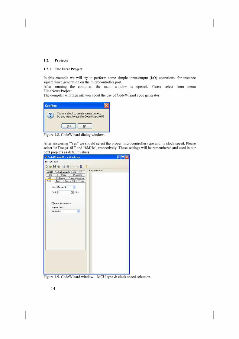
1.2. Projects
1.2.1. The First Project
In this example we will try to perform some simple input/output (I/O) operations, for instance
square wave generation on the microcontroller port.
After running the compiler, the main window is opened. Please select from menu
File>New>Project.
The compiler will then ask you about the use of CodeWizard code generator:
Figure 1.8. CodeWizard dialog window.
After answering “Yes” we should select the proper microcontroller type and its clock speed. Please
select “ATmega16L” and “8MHz”, respectively. These settings will be remembered and used in our
next projects as default values.
Figure 1.9. CodeWizard window – MCU type & clock speed selection.
14
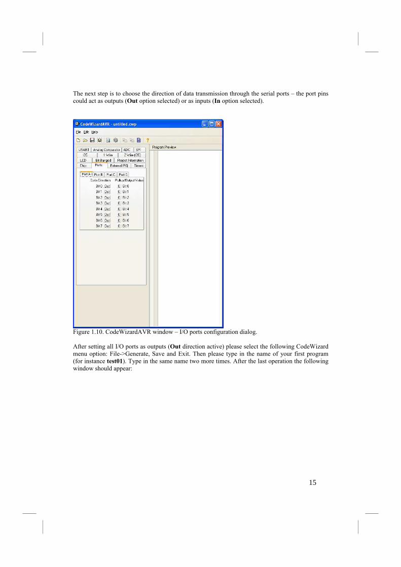
The next step is to choose the direction of data transmission through the serial ports – the port pins
could act as outputs (Out option selected) or as inputs (In option selected).
Figure 1.10. CodeWizardAVR window – I/O ports configuration dialog.
After setting all I/O ports as outputs (Out direction active) please select the following CodeWizard
menu option: File->Generate, Save and Exit. Then please type in the name of your first program
(for instance test01). Type in the same name two more times. After the last operation the following
window should appear:
15
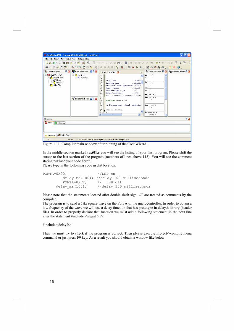
Figure 1.11. Compiler main window after running of the CodeWizard.
In the middle section marked text01.c you will see the listing of your first program. Please shift the
cursor to the last section of the program (numbers of lines above 115). You will see the comment
stating “//Place your code here”.
Please type in the following code in that location:
PORTA=0X00; //LED on delay_ms(100); //delay 100 milliseconds PORTA=0XFF; // LED off delay_ms(100); //delay 100 milliseconds
Please note that the statements located after double slash sign “//” are treated as comments by the
compiler.
The program is to send a 5Hz square wave on the Port A of the microcontroller. In order to obtain a
low frequency of the wave we will use a delay function that has prototype in delay.h library (header
file). In order to properly declare that function we must add a following statement in the next line
after the statement #include <mega16.h>
#include <delay.h>
Then we must try to check if the program is correct. Then please execute Project->compile menu
command or just press F9 key. As a result you should obtain a window like below:
16
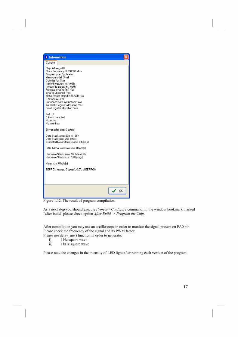
Figure 1.12. The result of program compilation.
As a next step you should execute Project->Configure command. In the window bookmark marked
“after build” please check option After Build -> Program the Chip.
After compilation you may use an oscilloscope in order to monitor the signal present on PA0 pin.
Please check the frequency of the signal and its PWM factor.
Please use delay_ms() function in order to generate:
i) 1 Hz square wave
ii) 1 kHz square wave
Please note the changes in the intensity of LED light after running each version of the program.
17

1.2.2. The Second Project
A paced loop
This project will help us to understand the practical applications of the binary and hexadecimal
numerical systems. In this example we will try to define an 8-bit software counter (using a single
byte char type variable) and transfer its contents to I/O port. Please close the previous project; next generate a new one (the detailed procedure was described
above). Please use CodeWizardAVR and select the name of project test02 (or any other name of
your choice).
The following code will commence this task (for sake of brevity only the crucial parts of the
program were listed):
#include <delay.h> //delay functions library declaration unsigned char counter; // an 8-bit variable called counter
….
while (1) { // Place your code here PORTA=~counter; //bitwise negation of the I/O port delay_ms(100); // 100 ms delay counter++; //counter incrementation };
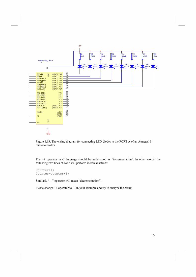
Before compiling this code we should connect 8 LED diodes to the output pins of the
microcontroller according to the following circuit diagram shown in Fig.1.13.
Please note that the bitwise negation (~ operator) of the counter variable is performed in order to obtain the lighting up of the LED diodes signaling the 1 (high) state. Without that modification
only the positions connected to ports lines in “0” (Low) state would light up the relevant LED
diode. After the modification the logic level “1” (high) states present on the PORT A output pins
are displayed by lighted LED diodes.
Please also note that only decimal numbers from the range 0..255 (00000000..11111111 in binary
format) can be displayed that way – after reaching the maximal value the counter variable is reset
back to zero. As a general rule, the n-bit variable may contain values from 0 to 2n-1 decimal (where
n is an integer positive number).
18
AGND31
X1
X2
RESET
PD2 (INT0)PD3 (INT1)PD4 (OC1B)PD5 (OC1A)
PB0 (T0)PB1 (T1)PB2 (AIN0)PB3 (AIN1)PB4 (SS)PB5 (MOSI)PB6 (MISO)PB7 (SCK)
(ADC0) PA040
(ADC1) PA139
(ADC2) PA238
(ADC3) PA337
(ADC4) PA436
(ADC5) PA535
(ADC6) PA634
(ADC7) PA733
PC022
PC123
PC224
PC325
PC426
PC527
(TOSC1) PC628
(TOSC2) PC729
PD7 (TOSC2)PD6 (ICP)
AVCC30
AREF32
PD1 (TXD)PD0 (RXD)
GND
11VCC
10
U1ATMEGA16_DIP40
D1LED
D2LED
D3LED
D4LED
D5LED
D6LED
D7LED
D8LED
R1680R
R2680R
R3680R
R4680R
R5680R
R6680R
R7680R
R8680R
+5V
GND
Figure 1.13. The wiring diagram for connecting LED diodes to the PORT A of an Atmega16
microcontroller.
The ++ operator in C language should be understood as “incrementation”. In other words, the
following two lines of code will perform identical actions:
Counter++; Counter=counter+1;
Similarly “-- ” operator will mean “decrementation”.
Please change ++ operator to - - in your example and try to analyze the result.
19

1.2.3. The Third project
An LCD display routines
An HD44780 Character LCD is a de facto industry standard liquid crystal display (LCD) display
device designed for interfacing with embedded systems. These screens come in a variety of
configurations including 8x1, which is one row of eight characters, 16x2, and 20x4.
These LCD screens are limited to text only and are often used in copiers, fax machines, laser
printers, industrial test equipment, networking equipment such as routers and storage devices.
Character LCDs can come with or without backlights, which may be LED, fluorescent, or
electroluminescent.
Character LCDs use a standard 14-pin interface and those with backlights have 16 pins. The pinouts
are as follows:
1. Ground
2. VCC (+3.3 to +5V)
3. Contrast adjustment (VO or VLC)
4. Register Select (RS). RS=0: Command, RS=1: Data
5. Read/Write (R/W). R/W=0: Write, R/W=1: Read
6. Clock (Enable). Falling edge triggered
7. Bit 0 (Not used in 4-bit operation)
8. Bit 1 (Not used in 4-bit operation)
9. Bit 2 (Not used in 4-bit operation)
10. Bit 3 (Not used in 4-bit operation)
11. Bit 4
12. Bit 5
13. Bit 6
14. Bit 7
15. Backlight Anode (+)
16. Backlight Cathode (-)
There may also be a single backlight pin, with the other connection via Ground or VCC pin. The
two backlight pins may precede the pin 1.
The nominal backlight voltage is around 4.2V at 25˚C using a VDD 5V capable model.
Character LCDs can operate in 4-bit or 8-bit mode. In 4 bit mode, pins 7 through 10 are unused and
the entire byte is sent to the screen using pins 11 through 14 by sending 4-bits (nibble) at a time.
The Gotronik AVR board includes a HD4470 compatible LCD display (2 lines, 16 characters per
line).
Please start CodeVision AVR C compiler. After the start-up the compiler should open the window
containing the last project. We should close it with File->Close All command. Then we should
create a new project from a scratch using File->�ew command (then please check project radio
button). The compiler will ask about the usage of CodeWizardAVR – please answer “Yes”. Then
the window of CodeWizardAVR should open.
20
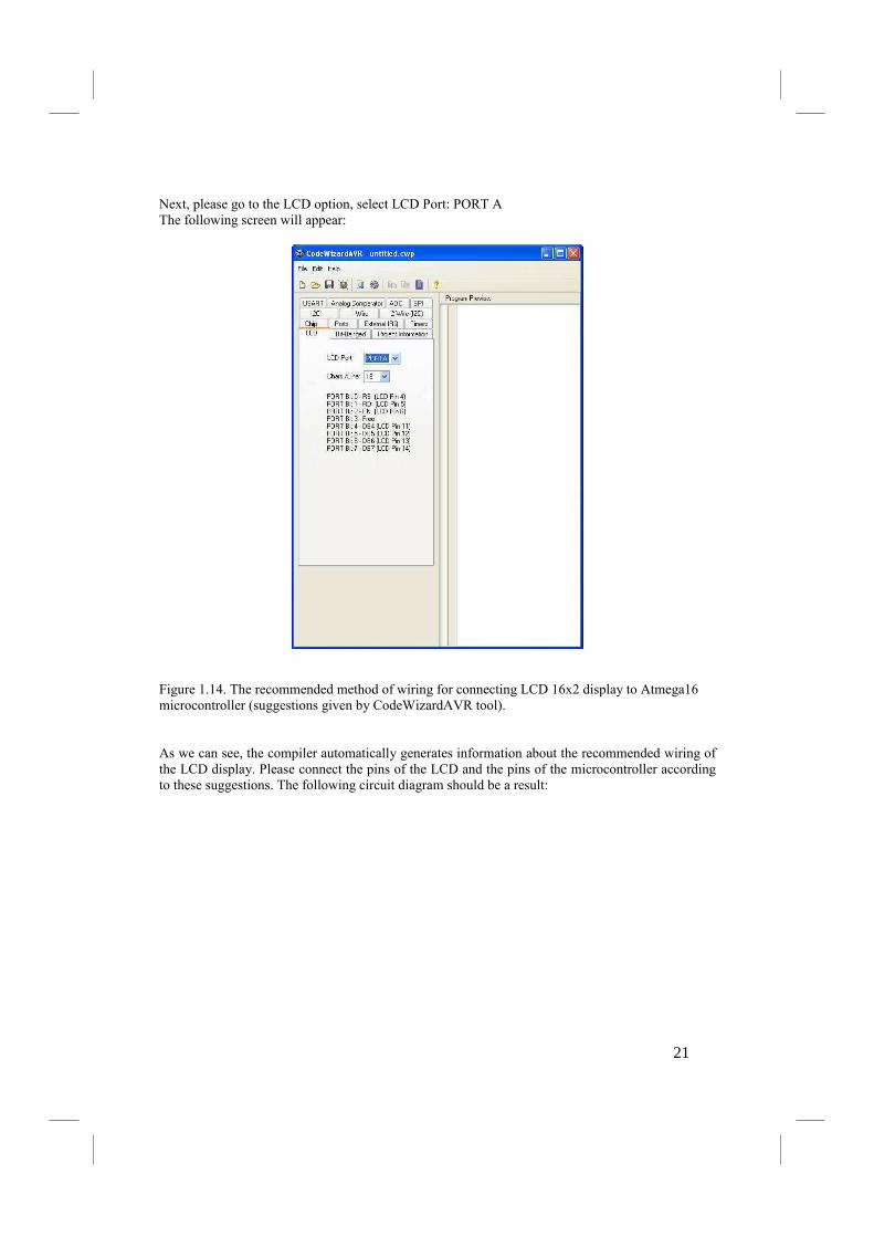
Next, please go to the LCD option, select LCD Port: PORT A
The following screen will appear:
Figure 1.14. The recommended method of wiring for connecting LCD 16x2 display to Atmega16
microcontroller (suggestions given by CodeWizardAVR tool).
As we can see, the compiler automatically generates information about the recommended wiring of
the LCD display. Please connect the pins of the LCD and the pins of the microcontroller according
to these suggestions. The following circuit diagram should be a result:
21

VSS1
VDD2
VLC3
RS4
RW5
E6
DB07
DB18
DB29
DB310
DB411
DB512
DB613
DB714
VLED15
VLED_GND16
HD44780
AGND31
X1
X2
RESET
PD2 (INT0)PD3 (INT1)PD4 (OC1B)PD5 (OC1A)
PB0 (T0)PB1 (T1)PB2 (AIN0)PB3 (AIN1)PB4 (SS)PB5 (MOSI)PB6 (MISO)PB7 (SCK)
(ADC0) PA040
(ADC1) PA139
(ADC2) PA238
(ADC3) PA337
(ADC4) PA436
(ADC5) PA535
(ADC6) PA634
(ADC7) PA733
PC022
PC123
PC224
PC325
PC426
PC527
(TOSC1) PC628
(TOSC2) PC729
PD7 (TOSC2)PD6 (ICP)
AVCC30
AREF32
PD1 (TXD)PD0 (RXD)
GND
11VCC
10
U1
ATMEGA16_DIP40
GND
VCC
LCD DISPLAY16 CHARACTERS X 2 LINES
Figure 1.15. The wiring diagram for connecting LCD 16x2 display to atmega16 microcontroller.
Please note that CodeVision compiler uses slightly different names for LCD pins (RD instead of
RW, E instead of EN).
Next please generate the program code (Generate, Save and Exit option from CodeWizardAVR
window). The compiler will prompt you for the name of your file: please enter prog03 or any name
of your choice, then repeat the name two more times. Then a template file should be generated and
opened in the main (editor) window. Please note that at about line 26 the declarations concerning
LCD display are generated:
// Alphanumeric LCD Module functions #asm .equ __lcd_port=0x1B ;PORTA #endasm #include <lcd.h>
The declarations include both the information about the I/O MCU port where the LCD was
connected and the information about the lcd.h library that will be necessary for programming LCD
displays based on HD44780 chip.
The last part of code should include the following text:
// LCD module initialization lcd_init(16); while (1) {
22

// Place your code here }; }
As usual, we should place our own code after the relevant comment (inside the last while loop). We should start with putting the following command inside the loop:
lcd_putchar(’A’);
Then please enter Project->Configure menu and select After Build bookmark, then select After
Build option and finally check “Program the chip” option. Then please execute Project->Build All
command. The project should be compiled and sent to the memory of the microcontroller, and then
the MCU will be restarted. The result of the execution of our program should be the filling of LCD
display with the letter ‘A’. W should see the following contents of the LCD screen:
Please note the cursor of the display is scrolled on the right just after the printing the next character
onto the LCD screen. In order to obtain only a single ‘A’ letter on the display we should move the
cursor back to the initial position. This task could be accomplished with lcd_gotoxy(x,y) command using the following coordinates:
As you can see, the X coordinate (values between 0 and 15) is related to the horizontal axis and the
Y coordinate (values 0 or 1 for two-line display) – the vertical axis. The reference point
(coordinates: 0,0) is located in the left upper corner of the LCD display.
Next, please modify your program in the following way:
while (1) { // Place your code here lcd_putchar('A'); // display a single character on LCD lcd_gotoxy(0,0); // move cursor back to the reference //point (0,0) }; }
After the compilation and running of the program we should see the following result:
The lcd_putchar() command used in the last example can be used only for displaying a single
character on an LCD screen. In case a longer text string is needed, Lcd_putsf() command should be utilized:
AAAAAAAAAAAAAAAA
AAAAAAAAAAAAAAAA
0,0 15,0
0,1 15,1
A
23

while (1) { // Place your code here lcd_gotoxy(0,0); lcd_putsf("Mechatronics"); lcd_gotoxy(0,1); lcd_putsf("Lab"); }; }
After compilation and execution of the last example the display should look like this:
Lcd_pusf() function displays at the current position a string stored in flash memory. Flash memory
is used here in order to save valuable locations in RAM memory (an amount of built-in Flash
memory is lower than RAM memory).
The main limitation of lcd_putsf() function is that it is only capable of displaying a constant text
string, i.e. lcd_putsf() function cannot be used for sending a result of measurement of computation
(or any other dynamic data) to the LCD display. To accomplish such a task a slightly more complex
procedure should be used.
To illustrate this we will write a code that will be incrementing the integer variable (starting from 0)
in the loop; during each iteration of the loop the current value of the variable will be displayed on
the LCD.
In order to commence the task, we should declare two variables. The first variable (of two-byte type
called int) will be called counter; the counted values will be stored there in binary format. The next variable will be a 6-byte buffer in RAM memory for storing the counted values after
conversion to the text string form (type char). The declaration should be located just after the comment “Declare your global variables here”.
// Declare your global variables here unsigned int counter; char buffer [6] ;
Please also add the declaration of the standard input-output library:
#include <stdio.h>
The declarations of the system libraries should be placed before the declarations of the variables.
The contents of the main while() loop are presented below (with comments starting from //signs):
Mechatronics
Lab
24

while (1) { // Place your code here lcd_gotoxy(0,0); //cursor at initial position lcd_putsf("Count = "); //display string “Count =” on the LCD
sprintf(buffer,"%u",counter); //convert the binary value of //counter variable to text form and store
// the result of the conversion in string variable “buffer” lcd_puts(buffer); //current value of the counter displayed in text form on LCD counter++; // increment the value of the counter delay_ms(10); // 10 ms delay before the next iteration lcd_clear(); //clear the contents of the LCD display };
After compiling and running the program we should see the dynamically changing contents of the
LCD display.
In place of the “xxxxx”, the current value is displayed in a decimal format. Please note that after
reaching the value of 65535 (the maximal value for two-byte int type variable) the counter is reset to zero. The contents of the counter are updated approximately every 10 milliseconds.
Please – as before – try to replace ++ operator with - - ; then try to analyze the result.
Count=xxxxx
25
1.2.4. The Fourth Project
A/D converter routines, sensor signal conditioning
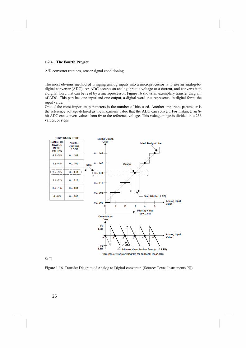
The most obvious method of bringing analog inputs into a microprocessor is to use an analog-to-
digital converter (ADC). An ADC accepts an analog input, a voltage or a current, and converts it to
a digital word that can be read by a microprocessor. Figure 16 shows an exemplary transfer diagram
of ADC. This part has one input and one output, a digital word that represents, in digital form, the
input value.
One of the most important parameters is the number of bits used. Another important parameter is
the reference voltage defined as the maximum value that the ADC can convert. For instance, an 8-
bit ADC can convert values from 0v to the reference voltage. This voltage range is divided into 256
values, or steps.
© TI
Figure 1.16. Transfer Diagram of Analog to Digital converter. (Source: Texas Instruments [5])
26
The size of the step for n-bit converter is given by a simple formula:
1 step = Vref/2n-1
The voltage value equivalent to 1 step is also called Least Significant Bit (LSB)
For n=10 and Vref=5V we obtain
1 LSB=5V/(210-1) = 5V/1023 = approx. 5mV
The analog-to-digital converter (ADC) found on the atMega MCU is a 10-bit successive
approximation device. There are a few important items that must be remembered when dealing with
the converter:
a) The inputs of the ADC share the common pins with I/O pins of PORTA. b) The ADC must be configured before using c) When reading we must remember that the A/D conversion time exceeds a few microseconds
(this may be vital during measurement of fast signals).
Before using ADC we should start a new project and open CodeWizardAVR. Then we should open
ADC bookmark and check “ADC Enabled” option. Please also select Auto Trigger Source = Free
Running.
After program generation we should include the following code inside the main while(1) loop:
27

Figure 17. CodeWizardAVR window – ADC configuration dialog
Include <stdio.h> Include <delay.h> Unsigned int result; Char buffer [6]; … while (1) { lcd_gotoxy(0,0); result=read_adc(0); // read voltage present at ADC0 input sprintf(buffer,"%u",result); // convert the result to //an integer value lcd_clear(); lcd_puts(buffer); delay_ms(200); }; }
28

After compilation and running the program we should see the dynamically changing contents of the
LCD display.
Instead the “xxxx”, a numerical value from the range 0000..1023 is displayed in a decimal format.
Please note that the readout is expressed in bits (for 10-bit converter the range is from 0 to 210-1).
In practical applications the more useful format of the measured signal value would be voltage. In
order to re-scale the bit-expressed values to volts we would need the following modifications:
float voltage_fp; // floating point variable declaration … while (1) { lcd_gotoxy(0,0); result=read_adc(0); // read voltage present at ADC0 input voltage_fp=(result*5.00)/1023; // convert the result to volts sprintf(buffer,"%5.3f",voltage_fp); //convert the voltage //value into a floating-point number and store it in buffer lcd_clear(); lcd_puts(buffer); delay_ms(200); }; }
The last example should produce the following result:
Where x.xxx is the measured voltage value expressed in volts (as a fixed-decimal point number).
Please note that the line: voltage_fp=(result*5.00)/1023; Converts voltage variable (int type) into a floating-point
And the next line of code: sprintf(buffer,"%5.3f",voltage_fp);
converts floating-point voltage_fp value into a text string format containing 5 digits stored in
format x.xxx (3 digits after the decimal point). The text string will be stored in buffer variable.
The A/D converter can be used for measurement of any analog signal, for instance for sensor signal
acquisition.
xxxx
x.xxx
29
The detailed explanation of an A/D converter operation is definitely beyond the scope of this book;
please refer for instance to an excellent application report published by Texas Instrument [5].
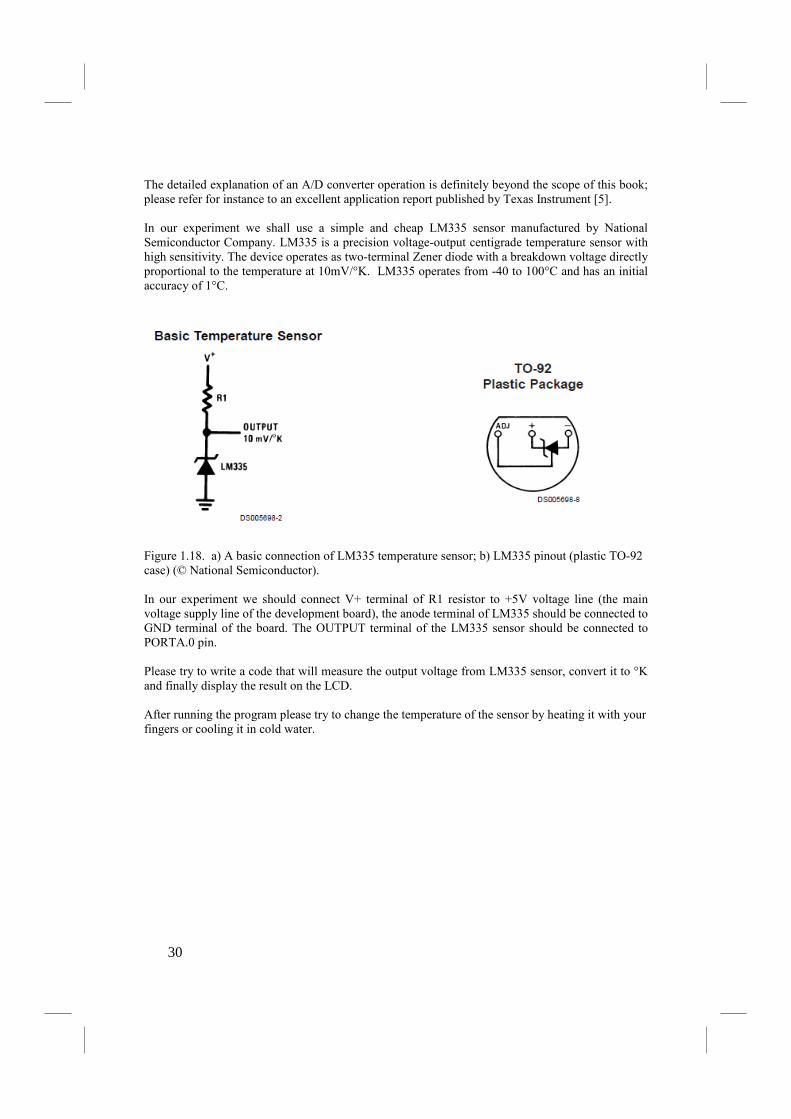
In our experiment we shall use a simple and cheap LM335 sensor manufactured by National
Semiconductor Company. LM335 is a precision voltage-output centigrade temperature sensor with
high sensitivity. The device operates as two-terminal Zener diode with a breakdown voltage directly
proportional to the temperature at 10mV/°K. LM335 operates from -40 to 100°C and has an initial
accuracy of 1°C.
Figure 1.18. a) A basic connection of LM335 temperature sensor; b) LM335 pinout (plastic TO-92
case) (© National Semiconductor).
In our experiment we should connect V+ terminal of R1 resistor to +5V voltage line (the main
voltage supply line of the development board), the anode terminal of LM335 should be connected to
GND terminal of the board. The OUTPUT terminal of the LM335 sensor should be connected to
PORTA.0 pin.
Please try to write a code that will measure the output voltage from LM335 sensor, convert it to °K
and finally display the result on the LCD.
After running the program please try to change the temperature of the sensor by heating it with your
fingers or cooling it in cold water.
30
1.2.5. The Fifth Project
Serial data transmission, USART programming.
One of the most important limitations met by the designers of embedded systems is the limited
number of I/O pins. The problem is especially important in the context of data transmission over
long distance, where the cost of cabling is also an important factor.
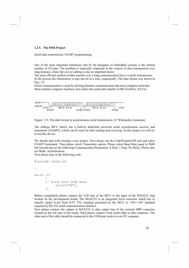
The most efficient method of data transfer over a long communication line is a serial transmission.
In the process the information is sent one bit at a time, sequentially. The data format was shown in
Fig.1.19.
Serial communication is used for all long-distance communication and most computer networks.
Most modern computer interfaces also utilize the serial data transfer (USB, FireWire, SATA).
Figure 1.19. The data format in asynchronous serial transmission. (© Wikimedia Commons).
The atMega MCU family has a built-in dedicated universal serial asynchronous receiver and
transmitter (USART), which can be used for data sending and receiving. In this project we will try
to use this device.
We should start with creating a new project. Next please run the CodeWizardAVR tool and select
USART bookmark. Then please check Transmitter option. Please select Baud Rate equal to 9600
bits/second and set the following Communication Parameters: 8 Data, 1 Stop, No Parity. Please also
set Mode: Asynchronous.
Next please type in the following code:
#include <stdio.h> … while (1) { // Place your code here printf("A"); };
Before compilation please connect the TxD line of the MCU to the input of the MAX232 chip
located on the development board. The MAX232 is an integrated level converter which has to
transfer signal levels from 0/5V TTL standard generated by the MCU to -10V/+10V standard
required by RS-232 serial communication interface.
Next please connect the output of MAX232 to data output line of the external DB9 connector
located on the left side of the board. Then please connect 9-pin serial cable to that connector. The
other end of the cable should be connected to the COM port socket in our PC computer.
31

Then please compile and run the program. Next please select Tools->Terminal option. In the lower
part of the screen a terminal window will open. Next please click the “Connect” button with the
mouse. In the terminal window a stream of data should appear. Please analyze the contents of the
transmission. Please also note that the data received by the PC are generated just by the MCU.
Figure 1.20. CodeWizardAVR window – USART configuration dialog
Next we should try to perform a voltage measurement using ADC and send the measured data over
the serial interface. In order to do so, please create a new project. Activate ADC and USART using
CodeVisionAVR. Then please insert the following code into the final While(1) loop :
#include <stdio.h> unsigned int result; char buffer [6]; … while (1) {
32
// Place your code here result=read_adc(0); sprintf (buffer,"%u",result); printf("%u\r",result); };
Next please compile and execute the program, then please activate the Terminal tool.
In the Terminal window we should see the consecutive results of the voltage measurement.
Please note that the transmitted data could be easily collected and stored in a disc file for future
analysis.
Literature:
[1] Atmel atMega16 MCU datasheet and application notes: www.atmel.com
[2] CodeVisionAVR User’s Manual http://www.hpinfotech.ro
[3] Barnett Richard H., Cox Sarah A., O'Cull Larry D. : Embedded C Programming and the Atmel
AVR (Second Edition), Delmar Cengage Learning, 2006, ISBN: 1418039594
[4] Kernighan; Dennis M. Ritchie. The C Programming Language (2nd ed.). Englewood Cliffs, NJ:
Prentice Hall. ISBN 0-13-110362-8. http://cm.bell-labs.com/cm/cs/cbook/.
(please note: the book was later replaced by “The ANSI C Programming Language”).
[5] Understanding Data Converters, TI Application Report SLAA013, www.ti.com
33

CPU2220 1 2 3 4 5 6 7
0 1 2 3 4 5
EM2220 1 2 3
0 1 2 3
Central Processing Unit
0 1 2 3 4 5 6 7
0 1 2 3 4 5
EM235 EM277
4
CPU Fault
Power
SIEMENS
Communication ModuleAnalog I/O ModuleDigital Output Module
2. Process automation using PLCs
2.1. Introduction
One of the more important demands for companies is placed on competitiveness [1]. The
main problem to solve is how to reduce manufacturing costs, while simultaneously improving the
quality, reliability, aesthetics, modernity and durability of products.
To reach these goals, appropriate methods of production management and optimization are
required, which is impossible without the implementation of control systems and robotics of the
process technologies.
Due to the wide range of tasks for modern control systems, applied devices should characterize such
features as universality, flexibility, reliability and accordance to obtains standards.
These requirements fit so-called Programmable Logic Controllers.
A Programmable Logic Controller (PLC) is a digital computer used for the automation of
miscellaneous processes, such as the control of machinery on factory assembly lines, amusement
rides, or lighting fixtures. PLCs are used in many industries and machines. Unlike general-purpose
computers, the PLC is designed for multiple inputs and output arrangements, extended temperature
ranges, immunity to electrical noise, and resistance to vibration and impact. Programs to control
machine operation are typically stored in battery-backed or non-volatile memory. A PLC is an
example of a real time system since output results must be produced in response to input conditions
within a bounded time, otherwise unintended operations will result [2].
2.2. Simatic S7-200 PLC
A popular example of PLC is Simatic S7-200 from Siemens. This device is intended for many
applications, among others in the chemical industry, chemical and plant engineering, diagnostics,
drug development, the food industry, electronics, energy industry, healthcare, the textile industry,
environmental technologies, waste management and recycling, and paints, coatings and inks. Of
course, it can be use in refrigeration and cryogenics processes too.
The S7-200 PLC is designed as consistently modular system and can be used as either a stand-alone
micro PLC solution or in conjunction with other controllers - its hardware configuration can be
modified in accordance to varying circumstances.
Fig. 2.1. An example of S7-200 hardware configuration
The modular system provides a range of specific expansions, for example, for temperature
measurement, weighting technology, positioning and communications [3].
The S7-200 Central Processing Unit (CPU) combines a microprocessor, an integrated 24V power
supply, input and output circuits, all in a compact housing [4], [5]. On the front panel the S7-200
34

Communications
port
Optional
cartridge
Status LEDs
- System Fault
- RUN
- STOP
Terminal
connector
I/O LEDs
Acces door
- mode selector
- analog potentiometer
- expansion port
contains the logic indicators required to monitor and control the input and output devices in
specified application (fig. 2.2).
Fig. 2.2. S7-200 CPU: front panel, indicators, controls and connectors.
The manufacturer provides several S7-200 CPU models with a diversity of features and capabilities
that help accommodate solutions for varied applications. Table 2.1 briefly compares the most
important features of available CPUs.
Table 2.1. Comparison of the S7-200 CPUs
Feature CPU 221 CPU222 CPU224 CPU224xp CPU226 Physical size [mm] 90x80x62 90x80x62 120,5x80x62 140x80x62 190x80x62 Program memory:
- with run mode edit
- without run mode edit
4096 bytes
4096 bytes
4096 bytes
4096 bytes
8192 bytes
12288 bytes
12288 bytes
16384 bytes
16384 bytes
24576 bytes
Data memory 2048 bytes 2048 bytes 8192 bytes 10240 bytes 10240 bytes Memory backup 50 hours
typical
50 hours
typical 100 hours
typical 100 hours
typical 100 hours
typical Local on-board I/O
- digital
- analog
6 IN/4 OUT
---
8 IN/6 OUT
---
14IN/10 OUT
---
14IN/10 OUT
2 IN/1 OUT
24IN/16 OUT
--- Expansion modules 0 2 7 7 7
High speed counters
- single phase
- two phase
4 at 30 kHz
2 at 20 kHz
4 at 30 kHz
2 at 20 kHz
6 at 30 kHz
4 at 20 kHz
4 at 30 kHz
2 at 200 kHz
3 at 20 kHz
1 at 100 kHz
6 at 30 kHz
4 at 20 kHz
Pulse outputs (DC) 2 at 20 kHz 2 at 20 kHz 2 at 20 kHz 2 at 100 kHz 2 at 20 kHz Analog adjustments 1 1 2 2 2
Real-time clock Cartridge Cartridge Built-in Built-in Built-in
Communications ports 1 x RS485 1 x RS485 1 x RS485 2 x RS485 2 x RS485 Floating-points math Yes
Digital I/O image size 256 (128 IN, 128 OUT)
Boolean execution speed 0,22 microseconds/instruction
For delivery process and application requirements, the S7-200 family can be equipped with many
expansion modules which add additional functionality to the S7-200 CPUs.
Table 2.2 shows a list of some available expansion modules.
35
Table 2.2. Expansion modules for the S7-200 CPU’s
Expansion
modules Type
Discrete modules
Input 8 x DC IN 8 x AC IN 16 x DC IN
Output 4 x DC OUT 4 x Relays 8 X Relays
8 x DC OUT 8 x AC OUT
Combination
4 x DC IN/
4 x DC OUT
8 x DC IN/
8 x DC OUT
16 x DC IN/
16 x DC OUT
32 x DC IN/
32 x DC OUT
4 x DC IN/
4 x Relay
8 x DC IN/
8 x Relay
16 x DC IN/
16 x Relay
32 x DC IN/
32 x Relay
Analog modules
Input 4 x Analog IN 8 x Analog IN 4 x Thermocouple
IN
2 x RTD IN
Output 2 x Analog OUT 4 x Analog OUT
Combination 4 x Analog IN/
4 x Analog OUT
Intelligent modules
Position Modem Profibus-DP
Ethernet Ethernet IT
Others
AS-Interface Siwarex
The Text Display (TD) device can also be connected to the S7-200 CPU. By means of Text
Display, monitor and change the process variables of controlled application is possible to view.
There are two programming options for connecting programming device (the most common
Personal Computer) to S7-200 CPU: connection with a Point-to-Point-Interface (PPI) Multi-Master
cable or a Communications Processor (CP) card with an Multi-Point-Interface (MPI) cable. The PPI
Multi-Master programming cable is the most common method of connecting PC to the S7-200
CPU. This cable connects the communications port of the S7-200 CPU (RS485) to the serial
communications of PC (RS232). The PPI Multi-Master programming cable can also be used to
connect other communications devices to the S7-200 CPU.
The STEP 7-Micro/WIN programming software (Fig. 2.3) allows developing, editing and
monitoring the algorithms for the application control using three types of program editors:
Statement List (STL), Ladder Diagram (LDR) and Function Block Diagram (FBD).
Fig. 2.3. An example of Step7-Micro/Win window with LDR editor
Others required descriptions and programming details are available in reference [6], [7], [8].
36
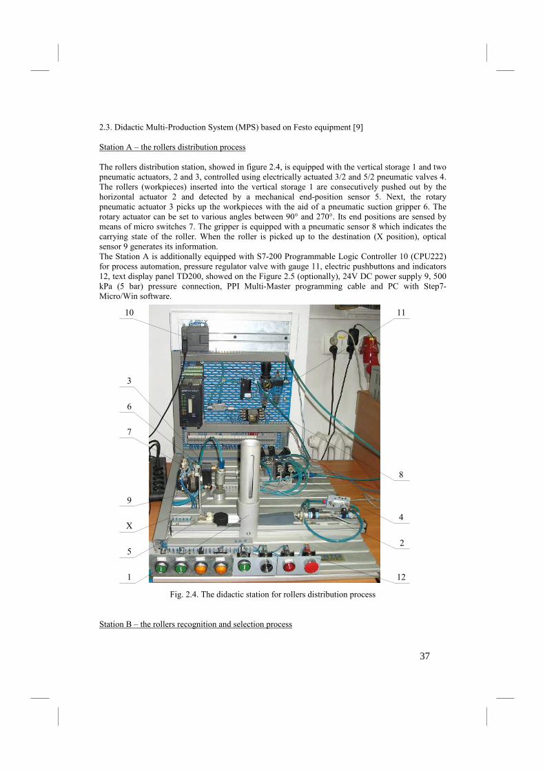
1
2
3
4
5
6
7
8
9
X
10 11
12
2.3. Didactic Multi-Production System (MPS) based on Festo equipment [9]
Station A – the rollers distribution process
The rollers distribution station, showed in figure 2.4, is equipped with the vertical storage 1 and two
pneumatic actuators, 2 and 3, controlled using electrically actuated 3/2 and 5/2 pneumatic valves 4.
The rollers (workpieces) inserted into the vertical storage 1 are consecutively pushed out by the
horizontal actuator 2 and detected by a mechanical end-position sensor 5. Next, the rotary
pneumatic actuator 3 picks up the workpieces with the aid of a pneumatic suction gripper 6. The
rotary actuator can be set to various angles between 90° and 270°. Its end positions are sensed by
means of micro switches 7. The gripper is equipped with a pneumatic sensor 8 which indicates the
carrying state of the roller. When the roller is picked up to the destination (X position), optical
sensor 9 generates its information.
The Station A is additionally equipped with S7-200 Programmable Logic Controller 10 (CPU222)
for process automation, pressure regulator valve with gauge 11, electric pushbuttons and indicators
12, text display panel TD200, showed on the Figure 2.5 (optionally), 24V DC power supply 9, 500
kPa (5 bar) pressure connection, PPI Multi-Master programming cable and PC with Step7-
Micro/Win software.
Fig. 2.4. The didactic station for rollers distribution process
Station B – the rollers recognition and selection process
37

1
3
2
4
5
6
7
8
9
10
11
12
The rollers recognition and selection station, shown in figure 2.5, is equipped with an identification
socket surrounded by three different sensors 1, two pneumatic actuators with end-position sensors,
2 and 3, controlled using electrically actuated 3/2 and 5/2 pneumatic valves 4 and the electric
conveyor 5.
The rollers inserted into the socket 1 are discerning by the sensors (differentiation between black or
non-black workpieces, metal or other stuff) and can exit the socket with the aid of horizontal
pneumatic actuator 2 or can be moved up using vertical pneumatic actuator 3 (lift). On this position,
the measurements of roller height using position sensor 6 and its accordance of color by means of
camera 7 are available. Next, the roller can be pushed out with the aid of a horizontal pneumatic
actuator 2 to onto conveyor 5, which can pick up its, for example to next station.
The Station B is additionally equipped with S7-200 Programmable Logic Controller 8 (CPU224)
for process automation, pressure regulator valve with gauge 9, electric pushbuttons and indicators
10, text display panel 11 (TD200), 24V DC power supply 12, 500 kPa (5 bar) pressure connection,
PPI Multi-Master programming cable and PC with Step7-Micro/Win software.
Fig. 2.5. The didactic station for rollers recognition and selection process
Station C – the rollers drilling process
The rollers drilling station, shown in figure 2.6, is equipped with the rotary table 1 with four sockets
2, electric drilling machine 3 mounted on the vertical pneumatic actuator (lift) 4, the vertical
pneumatic actuator 5, horizontal pneumatic actuator 6 and the optical presence sensor 7. All
pneumatic actuators are equipped with end-position sensors and are controlled using electrically
38
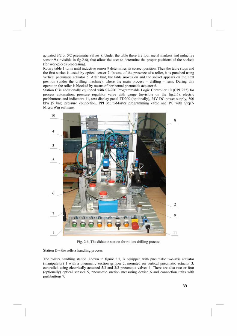
1
2
3
4
5
6
7
8
9
10
11
actuated 3/2 or 5/2 pneumatic valves 8. Under the table there are four metal markers and inductive
sensor 9 (invisible in fig.2.6), that allow the user to determine the proper positions of the sockets
(for workpieces processing).
Rotary table 1 turns until inductive sensor 9 determines its correct position. Then the table stops and
the first socket is tested by optical sensor 7. In case of the presence of a roller, it is punched using
vertical pneumatic actuator 5. After that, the table moves on and the socket appears on the next
position (under the drilling machine), where the main process – drilling – runs. During this
operation the roller is blocked by means of horizontal pneumatic actuator 6.
Station C is additionally equipped with S7-200 Programmable Logic Controller 10 (CPU222) for
process automation, pressure regulator valve with gauge (invisible on the fig.2.6), electric
pushbuttons and indicators 11, text display panel TD200 (optionally), 24V DC power supply, 500
kPa (5 bar) pressure connection, PPI Multi-Master programming cable and PC with Step7-
Micro/Win software.
Fig. 2.6. The didactic station for rollers drilling process
Station D – the rollers handling process
The rollers handling station, shown in figure 2.7, is equipped with pneumatic two-axis actuator
(manipulator) 1 with a pneumatic suction gripper 2, mounted on vertical pneumatic actuator 3,
controlled using electrically actuated 5/3 and 3/2 pneumatic valves 4. There are also two or four
(optionally) optical sensors 5, pneumatic suction measuring device 6 and connection units with
pushbuttons 7.
39

1 2 34
5
6
7
8
9
a. b.
The roller inserted into the marked place is detected by an optical sensor. The handling device picks
up the roller from there with the aid of a pneumatic gripper. The workpieces can be moved to three
available places according to defined criterion or can also be transferred to a downstream station (if
enabled).
Station D is additionally equipped with a portable set of S7-200 Programmable Logic Controller 8
(CPU222) for process automation, pressure regulator valve with gauge (invisible on fig.2.7), text
display panel TD200 (optionally), 24V DC power supply 9, 500 kPa (5 bar) pressure connection,
PPI Multi-Master programming cable and PC with Step7-Micro/Win software.
Fig. 2.7. The didactic station for rollers handling process
2.4. Laboratory tasks
2.4.1. Preliminary tasks
Task 1:
Create a pneumatic and electric diagram of your MPS and next, prepare an allocation list of inputs
and outputs of the PLC to the corresponding sensors and actuators.
Task 2:
Choose free buttons and an actuator from your MPS. Prepare relevant algorithms using Step7-
Micro/Win software to execute the diagrams shown below (use such functions, as contacts, coils,
timers, counters, etc.). Download consecutively your programs to the CPU and test its applications.
40
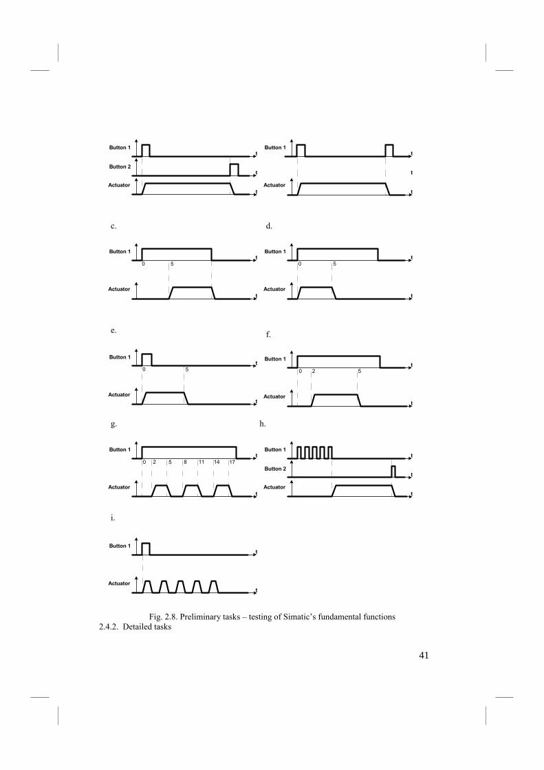
Button 1
Button 2
Actuator
t
t
t
Button 1
Actuator
t
t
50
Button 1
Actuator
t
t
50
Button 1
Actuator
t
t
50
Button 1
Actuator
t
t
520
Button 1
Actuator
t
t
52 8 11 14 170
Button 1
Button 2
Actuator
t
t
t
Button 1
Actuator
t
t
Button 1
Actuator
t
t
t
c. d.
e. f.
g. h.
i.
Fig. 2.8. Preliminary tasks – testing of Simatic’s fundamental functions
2.4.2. Detailed tasks
41

Be careful, in case of incorrect or unfinished program implemented in PLC, there is a risk of
serious injury!
Station A – the rollers distribution process
Load six different rollers (red, black and silver) to the storage. Develop a LDR diagram to solve the
following procedure.
The rollers are automatically pushed out from storage in case of free place on the position “X” (see
on the Fig.2.4). The TD200 panel shows current messages, describing state of process: ready to start
process, pushing out the roller, handling on the X position, the roller on the X position, black roller
on the X position, the storage is empty, amount of distributed rollers, full cycle time, etc. When the
process is stopped the TD 200 panel shows current status of the station or displays demo connected
with performing operations.
The task should be started and stopped alternatively by push the button mounted on the station or
using chosen function key (F1 …F8) on the text panel TD200.
Station B – the rollers recognition and selection process
Load free roller (red, black or silver) to the identification socket. Develop a LDR diagram to solve
the following procedure.
The roller is sensed by the sensors surrounding it. In case of black or red rollers, the workpiece
leaves out of the station. Otherwise the roller (silver) is moved up, where its height is measured.
Next, the roller is picked up on the conveyor whereby it leaves out of the station.
The TD200 panel shows current messages, describing the state of process: ready to start process -
the socket is empty, the roller in the socket, the result of the roller identification, leaving out or
handling upstairs of the roller, result of height measurement, moving by means of the conveyor,
amount of selected rollers, full cycle time, etc. When the process is stopped the TD 200 panel shows
the current status of the station or displays demo connected with performing operations.
The task should be started and stopped alternatively by pushing the button mounted on the station,
using the chosen function key (F1 …F8) on the text panel TD200 or automatically, respecting
required time delays for the operator’s safety.
Station C – the rollers drilling process
Load three rollers (red or silver) to the identification socket. Develop a LDR diagram to solve the
following procedure.
The rotary table starts and then stops, in all of four correct positions. During every stoppage, one
roller is blocking and drilling and concurrently the second is checking and punching. In case of the
absence of the roller, the drilling process during next stoppage isn’t performed.
The TD200 panel shows current messages, describing the state of process: ready to start process,
the socket is empty, presence of the roller, the drilling process is under way, the roller is ready for
collection, amount of drilled rollers, cycle time, speed of the drilling machine, etc. When the
process is stopped the TD 200 panel shows the current status of the station or displays demo
connected with performing operations.
The task should be started and stopped alternatively by pushing the button mounted on the station,
using the chosen function key (F1 …F8) on the TD200 text panel or automatically, respecting
required time delays for the operator’s safety. Additionally, by means of TD200 panel, the rotary
speed of the drilling machine should be controlled (using Pulse Wave Modulation function of the
PLC).
Station D – the rollers handling process
42

Load a red or silver roller to one of two enabled places for workpieces on the station. Develop a
LDR diagram to solve the following procedure.
The roller is automatically picked up to the second position, in case of a blank place. Consider
different algorithms of the rollers rearranged, when all four optical presence sensors are enabled.
The TD200 panel shows current messages, describing the state of process: ready to start process,
handling the roller, status of the places for the rollers (blank/engaged), amount of distributed rollers,
full cycle time, etc. When the process is stopped the TD 200 panel shows the current status of the
station or displays demo connected with performing operations.
The task should be started and stopped alternatively by pushing the button mounted on the station
or using the chosen function key (F1 …F8) on the text panel TD200.
Literature:
[1]. J. Swider, P. Michalski, G. Wszolek, Laboratory support for the didactic process of engineering
processes automation at the Faculty of Mechanical Engineering, Journal of Achievements in
Materials and Manufacturing Engineering, VOLUME 15, ISSUE 1-2, March-April, 2006
[2]. http://en.wikipedia.org
[3]. http://www.automation.siemens.com
[4]. http://www.allmar.pl, S7-200, Programmable Controller System Manual,
[5]. http://www.automation.siemens./solutionsandproducts/AS_1.htm
[6]. http://www.allmar.send.pl/upload/files/s7200/S7-200_manual_en.pdf
[7]. K. Kaminski, Programowanie w Step7-Micro/Win, wyd.3, Gryf
[8]. Micro automation Simatic S7-200, Siemens, Warszawa 2006
[9]. http://www.festo-didactic.com
43


![]µ Ì< Ì} }Á l] D X ] ol - UP · Nadprzewodniki na bazie *elaza w wietle bada metod spektroskopii mössbauerowskiej Artur B áachowski 1, Kamila Kom dera 1, Krzysztof Ruebenbauer](https://static.fdocuments.pl/doc/165x107/5fcb269d4dbf267ba66e03b2/-oe-oe-l-d-x-ol-up-nadprzewodniki-na-bazie-elaza-w-wietle-bada.jpg)