ARMScope – the versatile platform for scanning probe ...
12
Metrol. Meas. Syst., Vol. 27 (2020) No. 1, pp. 119–130 DOI: 10.24425/mms.2020.131711 METROLOGY AND MEASUREMENT SYSTEMS Index 330930, ISSN 0860-8229 www.metrology.pg.gda.pl ARMScope – THE VERSATILE PLATFORM FOR SCANNING PROBE MICROSCOPY SYSTEMS Bartosz Świadkowski, Tomasz Piasecki, Maciej Rudek, Michał Świ ˛ atkowski, Krzysztof Gajewski, Wojciech Majstrzyk, Michał Babij, Andrzej Dzierka, Teodor Gotszalk Wrocław University of Science and Technology, Faculty of Microsystem Electronics and Photonics, Janiszewskiego 11-17, 50-372 Wrocław, Poland ( [email protected], +48 71 320 3202, [email protected], [email protected], [email protected], [email protected], [email protected], [email protected], [email protected], [email protected]) Abstract Scanning probe microscopy (SPM) since its invention in the 80’s became very popular in examination of many different sample parameters, both in university and industry. This was the effect of bringing this technology closer to the operator. Although the ease of use opened a possibility for measurements without high labour requirement, a quantitative analysis is still a limitation in Scanning Probe Microscopes available on the market. Based on experience of Nano-metrology Group, SPM still can be considered as a tool for quantitative examination of thermal, electrical and mechanical surface parameters. In this work we present an ARMScope platform as a versatile SPM controller that is proved to be useful in a variety of applications: from atomic-resolution STM (Scanning Tunnelling Microscopy) to Multi-resonance KPFM (Kelvin Probe force microscopy) to commercial SEMs (Scanning electron microscopes). Keywords: Scanning probe microscopy, AFM, Kelvin Probe force microscopy, scanning tunnelling mi- croscopy. © 2020 Polish Academy of Sciences. All rights reserved 1. Introduction Scanning probe microscopy (SPM) belongs to the technologies enabling to examine electrical, thermal, optical and mechanical surface parameters. The basic idea of the SPM technology is to observe the so-called near-field interactions between the tip and the sample. SPM techniques have evolved significantly since their invention in the 80’s improving their capabilities and introducing new measurement modes [1]. In the last three decades SPM has become very popular in the university and industrial laboratories, mostly because of an enormous progress making this technology more user/operator-friendly and more reliable. Progress in the SPM technology can be identified in many fields. Copyright © 2020. The Author(s). This is an open-access article distributed under the terms of the Creative Commons Attribution- NonCommercial-NoDerivatives License (CC BY-NC-ND 4.0 https://creativecommons.org/licenses/by-nc-nd/4.0/), which permits use, dis- tribution, and reproduction in any medium, provided that the article is properly cited, the use is non-commercial, and no modifications or adaptations are made.
Transcript of ARMScope – the versatile platform for scanning probe ...

Metrol. Meas. Syst., Vol. 27 (2020) No. 1, pp. 119–130DOI: 10.24425/mms.2020.131711
METROLOGY AND MEASUREMENT SYSTEMS
Index 330930, ISSN 0860-8229www.metrology.pg.gda.pl
ARMScope – THE VERSATILE PLATFORM FOR SCANNING PROBEMICROSCOPY SYSTEMS
Bartosz Świadkowski, Tomasz Piasecki, Maciej Rudek, Michał Światkowski,Krzysztof Gajewski, Wojciech Majstrzyk, Michał Babij, Andrzej Dzierka, Teodor Gotszalk
Wrocław University of Science and Technology, Faculty of Microsystem Electronics and Photonics,Janiszewskiego 11-17, 50-372 Wrocław, Poland (B [email protected], +48 71 320 3202,[email protected], [email protected], [email protected],[email protected], [email protected], [email protected], [email protected],[email protected])
Abstract
Scanning probe microscopy (SPM) since its invention in the 80’s became very popular in examination ofmany different sample parameters, both in university and industry. This was the effect of bringing thistechnology closer to the operator. Although the ease of use opened a possibility for measurements withouthigh labour requirement, a quantitative analysis is still a limitation in Scanning Probe Microscopes availableon the market. Based on experience of Nano-metrology Group, SPM still can be considered as a tool forquantitative examination of thermal, electrical and mechanical surface parameters.In this work we present an ARMScope platform as a versatile SPM controller that is proved to be useful ina variety of applications: from atomic-resolution STM (Scanning Tunnelling Microscopy) to Multi-resonanceKPFM (Kelvin Probe force microscopy) to commercial SEMs (Scanning electron microscopes).
Keywords: Scanning probe microscopy, AFM, Kelvin Probe force microscopy, scanning tunnelling mi-croscopy.
© 2020 Polish Academy of Sciences. All rights reserved
1. Introduction
Scanning probe microscopy (SPM) belongs to the technologies enabling to examine electrical,thermal, optical and mechanical surface parameters. The basic idea of the SPM technology is toobserve the so-called near-field interactions between the tip and the sample. SPM techniques haveevolved significantly since their invention in the 80’s improving their capabilities and introducingnew measurement modes [1]. In the last three decades SPM has become very popular in theuniversity and industrial laboratories, mostly because of an enormous progress making thistechnology more user/operator-friendly and more reliable. Progress in the SPM technology canbe identified in many fields.
Copyright © 2020. The Author(s). This is an open-access article distributed under the terms of the Creative Commons Attribution-NonCommercial-NoDerivatives License (CC BY-NC-ND 4.0 https://creativecommons.org/licenses/by-nc-nd/4.0/), which permits use, dis-tribution, and reproduction in any medium, provided that the article is properly cited, the use is non-commercial, and no modifications oradaptations are made.

B. Świadkowski, T. Piasecki, et al.: THE VERSATILE PLATFORM FOR SCANNING PROBE. . .
Mechanical SPM heads are manufactured as rigid and compact components enabling highspeed surface scanning and immunity against vibration. Optical detectors of the tip displacementare designed as compact units making adjustments easier and more stable [2]. Also, resolution ofthe probe deflection in a range of tens of fm/Hz1/2 was presented [3].
The sample scanning is controlled by piezo-actuators integrated with external measurementunits determining the actuator position [4, 5]. The actuator resonance frequencies are increasingand thus making the video surface scanning possible [6–8]. In the SPM examinations a varietyof cantilevers integrated with various tips can be applied. They exhibit rigidity and changingresonance frequency in a range from 0.1 N/m up to 100 N/m and from 5 kHz up to 1 MHz,respectively. Tips of various shapes, including e.g. super sharp, high aspect ratio, sphere probesand tailored to chemical and/or physical properties can be applied in the sample examinations. Inthis way not only the surface topography is recorded but its chemical and physical properties aswell. The SPM applications span from microbiology and biotechnology up to material scienceand micro- and nano-electronics [9–12].
Despite enormous progress in this field several limitations of the SPM technology must beidentified as well. Difficulties in the metrology (in other words in the quantitative analysis) of therecorded phenomena and limited throughput of the surface analysis belong to the most importantones. In many publications the SPM metrology is associated with the so-called dimensionalmetrology but, based on the experience of the Nanometrology Division, the SPM techniquescan be applied in the quantitative examinations of thermal, electrical and mechanical surfaceparameters.
However, in this case the development of new scanning, control, data acquisition and signalprocessing schemes is almost always necessary. There are SPM systems available on the market,which are mostly optimized from the utilitarian point of view and are usually used as closedsystems. Their architecture provides the researcher with little space for the system modificationand its adaptation to the experimental requirements. In general, two classes of the microscopesetups can be distinguished. The first is the hardware-oriented one, which means that a varietyof system components can be applied to construct an instrument. However, in this case thepossibilities of implementing novel control and measurement algorithms are limited [13]. Thesecond class is the software-oriented one, which describes systems whose hardware environment isdefined [14]. They offer some flexibility which is however influenced by the hardware components.Additionally, the information describing the controller setup is usually supplied to promote theproduct from the marketing point of view and contains too little metrological data.
In our solution we are able to configure the hardware components in an arbitrary way and havethe full access to the software making it possible to define any control and measurement algorithm.It consists of three main functional blocks. The first one is a measurement head equipped witha probe assembly, a piezoelectric scanner with a sample holder and a micro-cantilever deflectiondetector (for AFM mode) or a tunnelling current detector (for STM mode). The SPM head isfixed on the vibration damping setup and enclosed in a noiseless chamber.
The second part is a modular ARMScope SPM controller. Its brain is a system controller con-taining an embedded microprocessor (ARM7-based) whose firmware controls the measurementand data acquisition processes. It communicates with exchangeable modules such as: analogue-to-digital converter (ADC) module, proportional – integral – derivative (PID) controllers, a scanfield controller or a stepper motor driver, by means of a dedicated system bus.
The third part is a user interface. The system controller communicates with the operator’sworkstation which is a typical personal computer at which the user uses a dedicated ARMScannerapplication to control the measurement process. A general view of the system’s components isshown in Fig. 1.
120

Metrol. Meas. Syst.,Vol. 27 (2020), No. 1, pp. 119–130DOI: 10.24425/mms.2020.131711
Fig. 1. A block diagram of ARMScope home-made scanning probe.
In this paper we present a so-called ARMScope platform, which makes it possible to performmetrological examinations of material and device nanostructure properties. The ARMScopeapplications span over standard topography measurements, multi-resonance Kelvin Probe forcemicroscopy (KPFM) [15], thermal examinations in the so-called load force modulation (LoFM)[14] and scanning tunnelling microscopy (STM) [17]. Various types of the tip-surface interactiondetectors have been applied in our experiments, which include optical beam deflection (OBD)detectors [15], piezo-resistive cantilevers [16] and electro-magnetic cantilevers [18]. The core ofthe system is the ARMScope controller, whose open and precisely defined architecture enablesto adapt the system to measurements performed at the atomic or hundreds of micrometre scalewith a scanning speed ranging from several to tens of lines per second. The architecture of theARMScope controller will be discussed in detail, especially the methodology of characterizationof the modules influencing the scanning and data acquisition process. These are the featuresof greatest importance for the development and application of the ARMScope controller in themetrological surface examinations.
2. ARMScope controller
2.1. System controller
In response to various needs of scanning probe microscopy, Nanometrology Division, Fac-ulty of Microsystem Electronics and Photonics, Wrocław University of Science and Technology,fabricated and tested a universal microscope controller, adjustable to different kinds of examina-tion, called ARMScope. During the design process, special attention was paid to modularity ofboth measurement electronics and control software. Specific functions were spread across easilyinterchangeable extension cards communicating with ARM (Advanced RISC Machine) MCU viaExternal Memory Interface (EMI). Modularity of the applied solution enables to use as manycards for control and signal acquisition as necessary to perform specific measurements. The em-bedded software has a modular structure that increases its portability to novel hardware solutions.The implemented functional blocks reduce the cost of extending its functionality. The systemcontroller is significantly supported by a home-made ARMScanner software and embedded soft-ware kit controlling the ARM microprocessor. The software architecture is based on a commoncommand pattern. Separated parts of the system communicate with ARM MCU using a definedset of commands. As a result of user actions, a related set of commands is created in the userinterface (ARMScanner). Using a dedicated transmission protocol, the settings are transmittedvia USB interface. The protocol block of the system controller’s firmware is responsible fordecoding and analysing (e.g. verifying its correctness) incoming data frames. Depending on the
121

B. Świadkowski, T. Piasecki, et al.: THE VERSATILE PLATFORM FOR SCANNING PROBE. . .
command type, the interrelated block of the controller is initialized and configured. The scanningprocess requires simultaneous signal generation and sampling. These functions are divided intwo independent software blocks. The time-control block uses high-resolution hardware timers toprovide necessary synchronization between other software modules. The block’s behaviour is setwith respect to the user-defined data that determine the positioning signal shape, timing, as wellas sampling type. When all blocks are set, the execution module can be triggered which starts thewhole process.
The PC software is the interface between the user and the MCU, enabling to change themeasurement modes as well as their parameters. It is also responsible for the analysis of theresults providing an online preview and correction of the measured sample property. AmongARMScanner’s up-to-date features the most important are: supporting multiple measurementmodes including sine and vector scanning, online image processing with a built-in module, errordetection, multithreading and a very convenient and precise positioning system with intelligentnavigation. In the vector scanning mode, which is one of the ARMScanner’s newest features, theprobe is moved according to any user-created pattern. Because of that, the overall path of the tipis shorter and the scan can be faster.
The main part of ARMScope SPM controller is an LPC 2478 MCU (MicrocontrollerUnit) thatcoordinates operation of the whole system using a 16-bit parallel bus and provides communicationwith PC. Every SPM needs common basic functions, like scanning field control, data acquisitionand probe positioning, but there are also more advanced functions dedicated to a specific kind ofmeasurement.
ARMScope scanner versatility was proved in various applications in Nanometrology Divisionlaboratories. It is used as a controller of STM and AFM microscopes and was successfully appliedto acquire images from vulnerable SEM microscopes: Hitachi S-570 and Jeol JSM-35.
2.2. Scan field controller
ARMScope controller is equipped with a dedicated Scan Field Controller. It consists of sixDACs in total and an analogue section for scaling and rotation, which is a combination of digitallycontrolled potentiometers and adders. Its schematic is shown in Fig. 2. Its role is to convert thespace of image coordinates into the space of sample coordinates (Fig. 2 – right) as:
xs = x0 + k × cos(α) × x − k × sin(α) × y, (1)
yS = y0 + k × cos(α) × y + k × sin(α) × x, (2)
where xs , ys are the coordinates in the sample space, x, y are the coordinates in the image space,k is a scaling factor, x0, y0 are offsets in the space of sample coordinates and α is the rotation
a) b)
Fig. 2. A block diagram of the rotation and scaling section of the Scan field controller module (left)and a visualisation of sample transformation to the space of image coordinates (right).
122
Metrol. Meas. Syst.,Vol. 27 (2020), No. 1, pp. 119–130DOI: 10.24425/mms.2020.131711
angle. Thanks to the analogue rotation and scaling section, the system ensures the capacity ofeasy sample imaging manipulation without any loss in resolution and noise performance.
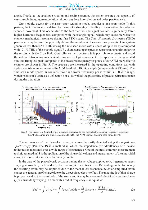
Our module, except for a classic raster scanning mode, provides a sine scan mode. In thispattern, the fast scan axis is driven by means of a sine signal, leading to a smoother piezoelectricscanner movement. This occurs due to the fact that the sine signal contains significantly fewerhigher harmonic frequencies, compared with the triangle signal, which may cause piezoelectricelement mechanical resonance during fast STM scans. The Total Harmonic Distortion (THD)parameter may be used to precisely define the number of harmonic components. Our systemgenerates less than 0.5% THD during the sine scan mode with a speed of up to 10 lps comparedwith 12.1% THD of the triangle signal. By characterizing the piezoelectric scanner and comparingthe results with the Scan Field Controller output spectrum it is possible to estimate and avoidthe risk of introducing mechanical resonances of piezo-element. The spectra of the generatedsine and triangle signals compared to the measured frequency response of our AFM piezoelectricscanner are shown in Fig. 3. The spectra were measured in the operating conditions, i.e. witha piezoelectric scanner mounted in AFM head with HOPG sample (sample weight 230 mg). Thesine scan mode spectrum contains fewer and lower frequency peaks within a 100 kHz range,which results in a decreased deflection noise, as well as the possibility of piezoelectric resonanceduring the operation.
Fig. 3. The Scan Field Controller performance compared to the piezoelectric scanner frequency response:the AFM scanner and triangle scan mode (left), the AFM scanner and sine scan mode (right).
The resonances of the piezoelectric actuator may be easily detected using the impedancespectroscopy (IS). The IS is a method in which the impedance (or admittance) of a deviceunder test is measured over a wide range of frequencies. One of the most common measurementtechniques used in IS is the application of the sinusoidal voltage and measurement of the sinusoidalcurrent response at a series of frequency points.
In the case of the piezoelectric actuator having the ac voltage applied to it, it generates stressvarying sinusoidally in time due to the inverse piezoelectric effect. Depending on the frequencythe resulting strain may be amplified due to the mechanical resonance. Such an amplified straincauses the generation of charge due to the direct piezoelectric effect. The magnitude of that chargeis proportional to the magnitude of the strain and it may be measured electrically, as the chargeQ(t) sinusoidally varying in time with a radial frequency ω is equal to:
Q(t) =
∫
I(t)d t =
∫
I0 cos(ωt)d t =I0
ωsin(ωt) =
|Y |U0
ωsin(ωt), (3)
123

B. Świadkowski, T. Piasecki, et al.: THE VERSATILE PLATFORM FOR SCANNING PROBE. . .
where I(t) is the current; I0 is the magnitude of the current; Y is the measured admittance; U0 is
the magnitude of the applied voltage. Therefore, plotting|Y |
ωU0 it may be obtained a plot which
will enable to visualise the mechanical resonances of the piezoelectric actuator. In practice, themeasured admittance is also influenced by the displacement current of the piezoelectric actuatorbut in most cases its influence may be neglected.
The source of x and y signals are Analog Devices AD5546 16-bit DACs. The scan fieldarithmetic is implemented using 12-bit AD7398 DACs working as digital potentiometers. TheScan Field Controller is also equipped with multiple auxiliary 12- and 16-bit DAC channels helpfulin performing additional functions, such as sample biasing or spectroscopy measurements. Allanalogue outputs operate within a ±10 V range.
Using an 18-bit ADC module described in the following section and the procedure of noisefloor measurements, we determined the performance of DACs. Main X, Y outputs achieve up to−100 dBFS noise during the dynamic operation, while the static noise of polarization outputs isno higher than the ADC module’s input noise with a linearity error equal to 0.75% in the fullrange.
2.3. Analogue-to-digital converter (ADC) module
The whole analogue signal acquisition in the ARMScope controller is performed usingan ADC module based on the Linear Technologies LTC2348-18 low-noise, 8-channel, 18-bitsuccessive approximation ADC [2] controlled by the circuitry implemented in the FPGA (XilinxSPARTAN-3). The ADC is capable of up to 200 ksps simultaneous sampling of each of 8 channelsor up to 1 Msps sampling of a single channel. The ADC module has 8 differential voltage inputswith a±10 V range. As the regular SPM measurements usually do not require such a fast samplingrate, the ADC module uses hardware-implementedoversampling and averaging up to 128 samplesto improve the resolution.
The performance of the ADC module was evaluated by measuring the noise floor whichlimits the small-signal resolution. The results are shown in Fig. 4. Without averaging the standarddeviation of samples is less than 1.5 bits which corresponds to −105 dBFS (magnitude referencedto the full-scale voltage) noise floor and 165 µV resolution. The use of averaging improves theseparameters up to −126 dBFS and 12.5 µV, respectively.
Fig. 4. The ADC module performance evaluated basing on the analysis of 216 samples: histograms and Gaussiandistribution curves using 128× and no averaging expressed in bits of resolution of the 18-bit ADC (left), noisefloor expressed relative to the full scale voltage and a resulting voltage resolution of the ADC module at a ±10 V
range (right).
124
Metrol. Meas. Syst.,Vol. 27 (2020), No. 1, pp. 119–130DOI: 10.24425/mms.2020.131711
2.4. PID controller
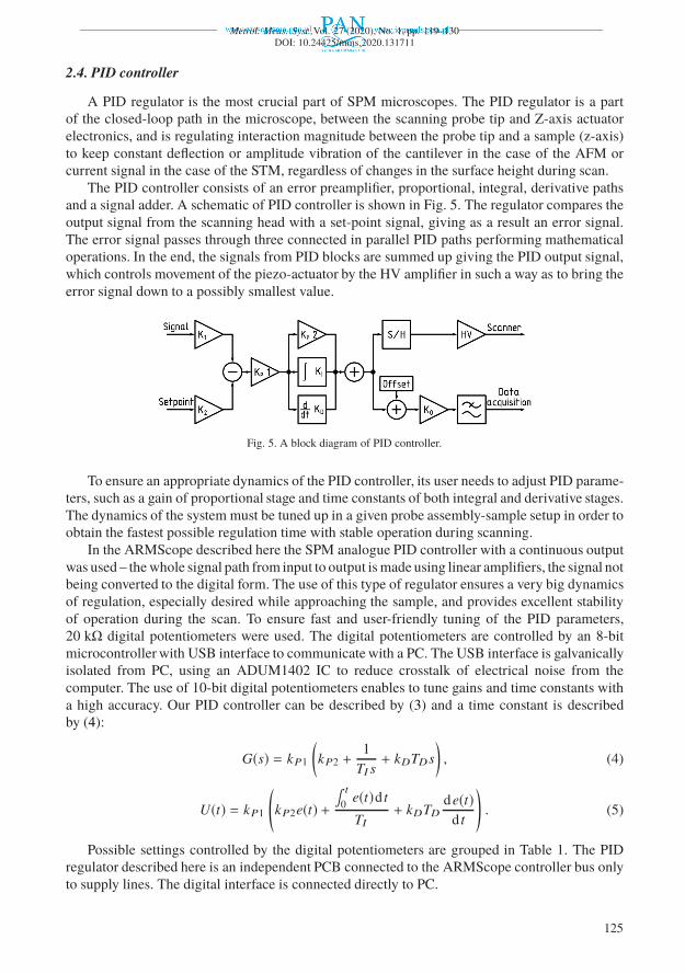
A PID regulator is the most crucial part of SPM microscopes. The PID regulator is a partof the closed-loop path in the microscope, between the scanning probe tip and Z-axis actuatorelectronics, and is regulating interaction magnitude between the probe tip and a sample (z-axis)to keep constant deflection or amplitude vibration of the cantilever in the case of the AFM orcurrent signal in the case of the STM, regardless of changes in the surface height during scan.
The PID controller consists of an error preamplifier, proportional, integral, derivative pathsand a signal adder. A schematic of PID controller is shown in Fig. 5. The regulator compares theoutput signal from the scanning head with a set-point signal, giving as a result an error signal.The error signal passes through three connected in parallel PID paths performing mathematicaloperations. In the end, the signals from PID blocks are summed up giving the PID output signal,which controls movement of the piezo-actuator by the HV amplifier in such a way as to bring theerror signal down to a possibly smallest value.
Fig. 5. A block diagram of PID controller.
To ensure an appropriate dynamics of the PID controller, its user needs to adjust PID parame-ters, such as a gain of proportional stage and time constants of both integral and derivative stages.The dynamics of the system must be tuned up in a given probe assembly-sample setup in order toobtain the fastest possible regulation time with stable operation during scanning.
In the ARMScope described here the SPM analogue PID controller with a continuous outputwas used – the whole signal path from input to output is made using linear amplifiers, the signal notbeing converted to the digital form. The use of this type of regulator ensures a very big dynamicsof regulation, especially desired while approaching the sample, and provides excellent stabilityof operation during the scan. To ensure fast and user-friendly tuning of the PID parameters,20 kΩ digital potentiometers were used. The digital potentiometers are controlled by an 8-bitmicrocontroller with USB interface to communicate with a PC. The USB interface is galvanicallyisolated from PC, using an ADUM1402 IC to reduce crosstalk of electrical noise from thecomputer. The use of 10-bit digital potentiometers enables to tune gains and time constants witha high accuracy. Our PID controller can be described by (3) and a time constant is describedby (4):
G(s) = kP1
(
kP2 +1
TI s+ kDTDs
)
, (4)
U(t) = kP1
(
kP2e(t) +
∫ t
0e(t)d t
TI
+ kDTD
de(t)
d t
)
. (5)
Possible settings controlled by the digital potentiometers are grouped in Table 1. The PIDregulator described here is an independent PCB connected to the ARMScope controller bus onlyto supply lines. The digital interface is connected directly to PC.
125

B. Świadkowski, T. Piasecki, et al.: THE VERSATILE PLATFORM FOR SCANNING PROBE. . .
Table 1. Digitally set parameters of PID Controller.
Parameter Unit Minimum value Maximum value
KP1 V/V 0.0476 1
KP2 V/V 0.0536 0.9464
TI for STM (CI = 68 nF) s 0.0112 1.50722
TI for AFM (CI = 100 nF) s 0.0165 2.2165
KD V/V 0.0536 0.9464
TD (CI = 10 nF) s 0.0015 0.2015
An example of PID open-loop output function as a result of intentionally modulated input ispresented in Fig. 6.
Fig. 6. The step-response open-loop output of PID regulator with an integral branch gain set to100%, a proportional branch gain set to 100% and a derivative branch gain set to 75%. Integratorand differentiator circuits have capacitances CI = CD = 10 nF. PID regulator parameters that can
be estimated: Ti = 300 µs, Kp100% = 1 V/V.
2.5. High-voltage driver section
Scanning Probe Microscope uses piezo-elements to position the micro-cantilever above thesample with a high accuracy and to control the magnitude of interactions (e.g. the force appliedbetween the tip and the sample or the tunnelling current amplitude). The home-made ARMScopeSPM is equipped with the custom-made piezo-tube-based scanner.
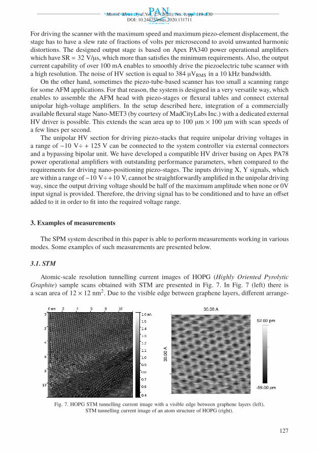
To apply in the STM system, our piezo-tube scanner has the maximum scan area of 100 nm×100 nm. Scans with a subatomic resolution require a high speed of movement. Our solutionachieved up to 85 lines per second, which is enough for imaging graphene membranes (Fig. 7).
Our standard AFM scanner provides a displacement in the area up to 15 µm × 15 µm drivenwith a bipolar±150 V. For driving such an actuator, we designed a compact high-voltage amplifier,which is part of ARMScope controller. This module has the form of an add-on board mountedonto the PID regulator circuit in order to enhance the noise performance of the Z-axis electricalcontrol path. The module consists of three independent functional blocks to control X , Y andZ axes. Furthermore, all channels have a switched gain of 1 V/V and 10 V/V, which enables toenhance resolution of topography scans onto sub-nanometre details or to increase the scan area.
126
Metrol. Meas. Syst.,Vol. 27 (2020), No. 1, pp. 119–130DOI: 10.24425/mms.2020.131711
For driving the scanner with the maximum speed and maximum piezo-element displacement, thestage has to have a slew rate of fractions of volts per microsecond to avoid unwanted harmonicdistortions. The designed output stage is based on Apex PA340 power operational amplifierswhich have SR = 32 V/µs, which more than satisfies the minimum requirements. Also, the outputcurrent capability of over 100 mA enables to smoothly drive the piezoelectric tube scanner witha high resolution. The noise of HV section is equal to 384 µVRMS in a 10 kHz bandwidth.
On the other hand, sometimes the piezo-tube-based scanner has too small a scanning rangefor some AFM applications. For that reason, the system is designed in a very versatile way, whichenables to assemble the AFM head with piezo-stages or flexural tables and connect externalunipolar high-voltage amplifiers. In the setup described here, integration of a commerciallyavailable flexural stage Nano-MET3 (by courtesy of MadCityLabs Inc.) with a dedicated externalHV driver is possible. This extends the scan area up to 100 µm × 100 µm with scan speeds ofa few lines per second.
The unipolar HV section for driving piezo-stacks that require unipolar driving voltages ina range of −10 V÷ + 125 V can be connected to the system controller via external connectorsand a bypassing bipolar unit. We have developed a compatible HV driver basing on Apex PA78power operational amplifiers with outstanding performance parameters, when compared to therequirements for driving nano-positioning piezo-stages. The inputs driving X, Y signals, whichare within a range of−10 V÷+10 V, cannot be straightforwardly amplified in the unipolar drivingway, since the output driving voltage should be half of the maximum amplitude when none or 0Vinput signal is provided. Therefore, the driving signal has to be conditioned and to have an offsetadded to it in order to fit into the required voltage range.
3. Examples of measurements
The SPM system described in this paper is able to perform measurements working in variousmodes. Some examples of such measurements are presented below.
3.1. STM
Atomic-scale resolution tunnelling current images of HOPG (Highly Oriented PyrolyticGraphite) sample scans obtained with STM are presented in Fig. 7. In Fig. 7 (left) there isa scan area of 12 × 12 nm2. Due to the visible edge between graphene layers, different arrange-
Fig. 7. HOPG STM tunnelling current image with a visible edge between graphene layers (left),STM tunnelling current image of an atom structure of HOPG (right).
127

B. Świadkowski, T. Piasecki, et al.: THE VERSATILE PLATFORM FOR SCANNING PROBE. . .
ments of atoms can be observed. Atoms in the upper part of the image are packed in parallel to thetop edge of the image, while atoms in the lower part of Fig. 7 are arranged in an angle in relationto the bottom edge of the image. In Fig. 7 (right), a clear atom structure of HOPG obtained inambient air is presented.
3.2. Topography measurements
The contact mode is the basic mode of AFM operation, where the tip is in continuous contactwith the sample. The cantilever deflection is set by the user and is related to the contact forcebetween the tip and the surface. Therefore, soft cantilevers (k < 1 N/m) are preferred to avoidunintentional sample damage during measurement. The cantilever deflection is controlled by PIDcontroller while the probe is moving above the scanned sample surface. In Fig. 8 images of HOPGand 6H-SiC (SiC/1.5 manufactured by TipsNano) samples are shown.
Fig. 8. An AFM image of HOPG sample obtained with Cont-PPP probes. A topography image of HOPG, scan area3.6 × 3.6 µm2 (top left), cross-section marked (top left) as “1”; atomic steps can be distinguished (bottom left).A topography image of silicon carbide, scan area 2.5×2.5 µm2 (top right), cross-section marked (top right) as “1”;
structural steps can be distinguished (bottom right).
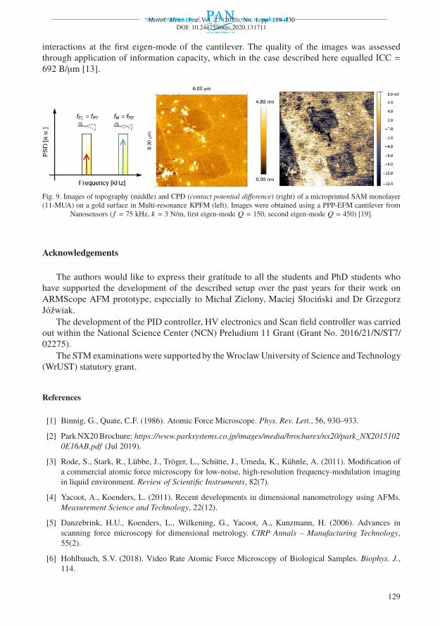
3.3. Multi-resonance KPFM
Multi-resonance KPFM enables to separate mechanical actuation frequency and electrostaticcarrier frequency in the non-contact mode. In the setup described here, it is possible to controlcantilever oscillation in the second eigen-mode while measuring and controlling electrostatic
128
Metrol. Meas. Syst.,Vol. 27 (2020), No. 1, pp. 119–130DOI: 10.24425/mms.2020.131711
interactions at the first eigen-mode of the cantilever. The quality of the images was assessedthrough application of information capacity, which in the case described here equalled ICC =692 B/µm [13].
Fig. 9. Images of topography (middle) and CPD (contact potential difference) (right) of a microprinted SAM monolayer(11-MUA) on a gold surface in Multi-resonance KPFM (left). Images were obtained using a PPP-EFM cantilever from
Nanosensors ( f = 75 kHz, k = 3 N/m, first eigen-mode Q = 150, second eigen-mode Q = 450) [19].
Acknowledgements
The authors would like to express their gratitude to all the students and PhD students whohave supported the development of the described setup over the past years for their work onARMScope AFM prototype, especially to Michał Zielony, Maciej Słociński and Dr GrzegorzJóźwiak.
The development of the PID controller, HV electronics and Scan field controller was carriedout within the National Science Center (NCN) Preludium 11 Grant (Grant No. 2016/21/N/ST7/02275).
The STM examinations were supported by the Wroclaw University of Science and Technology(WrUST) statutory grant.
References
[1] Binnig, G., Quate, C.F. (1986). Atomic Force Microscope. Phys. Rev. Lett., 56, 930–933.
[2] Park NX20 Brochure: https://www.parksystems.co.jp/images/media/brochures/nx20/park_NX20151020E16AB.pdf (Jul 2019).
[3] Rode, S., Stark, R., Lübbe, J., Tröger, L., Schütte, J., Umeda, K., Kühnle, A. (2011). Modification ofa commercial atomic force microscopy for low-noise, high-resolution frequency-modulation imagingin liquid environment. Review of Scientific Instruments, 82(7).
[4] Yacoot, A., Koenders, L. (2011). Recent developments in dimensional nanometrology using AFMs.Measurement Science and Technology, 22(12).
[5] Danzebrink, H.U., Koenders, L., Wilkening, G., Yacoot, A., Kunzmann, H. (2006). Advances inscanning force microscopy for dimensional metrology. CIRP Annals – Manufacturing Technology,55(2).
[6] Hohlbauch, S.V. (2018). Video Rate Atomic Force Microscopy of Biological Samples. Biophys. J.,114.
129

B. Świadkowski, T. Piasecki, et al.: THE VERSATILE PLATFORM FOR SCANNING PROBE. . .
[7] Ahmad, A., Ivanov, T., Angelov, T., Rangelow, I. (2015). Fast atomic force microscopy with self-transduced, self-sensing cantilever. J. Micro/Nanolith. MEMS MOEMS, 14(3).
[8] Ando, T. (2012). High-speed atomic force microscopy coming of age. Nanotechnology, 23(6).
[9] Szyszka, A., Obłak, M., Szymański, T., Wośko, M., Dawidowski, W., Paszkiewicz, R. (2016). Scanningcapacitance microscopy characterization of AIIIBV epitaxial layers. Mater. Sci. Pol., 34, 845–850.
[10] Dufrêne, Y.F., Ando, T., Garcia, R., Alsteens, D., Martinez-Martin, D., Engel, A., Müller, D.J. (2017).Imaging modes of atomic force microscopy for application in molecular and cell biology. NaturePublishing Group, 12.
[11] Alessandrini, A., Facci, P. (2005). AFM: A versatile tool in biophysics. Measurement Science andTechnology, 16(6).
[12] Janshoff, Neitzert, Oberdörfer, Fuchs (2000). Force Spectroscopy of Molecular Systems-SingleMolecule Spectroscopy of Polymers and Biomolecules. Angewandte Chemie, 39(18), 3212–3237.
[13] RHK product catalog: https://www.rhk-tech.com/r9plus/.
[14] Oxford Instruments catalog: https://afm.oxinst.com/products/mfp-3d-afm-systems/.
[15] Kopiec, D., Jóźwiak, G., Moczała, M., Sierakowski, A., Gotszalk, T. (2018). Multifrequency Kelvinprobe force microscopy on self assembled molecular layers and quantitative assessment of images’quality. Ultramicroscopy, 194, 100–107.
[16] Biczysko, P., Dzierka, A., Jóźwiak, G., Rudek, M., Gotszalk, T., Janus, P., Grabiec, P., Rangelow, I.W.(2018). Contact atomic force microscopy using piezoresistive cantilevers in load force modulationmode. Ultramicroscopy, 184(2018), 199–208.
[17] Gajewski, K., Kunicki, P., Sierakowski, A., Szymański, W., Kaczorowski, W., Niedzielski, P., Got-szalk, T. (2019). High-resolution, spatially-resolved surface potential investigations of high-strengthmetallurgical graphene using scanning tunnelling potentiometry. Microelectronic Engineering, 212,1–8.
[18] Świadkowski, B., Majstrzyk, W., et al. (2019). Near zero contact force atomic microscopy investigationsusing active electromagnetic cantilevers. submitted to Ultramicroscopy.
[19] Kopiec, D., Jóźwiak, G., Moczała, M., Sierakowski, A., Gotszalk, T. (2018). Multifrequency Kelvinprobe microscopy on self assembled molecular layers and quantitative assessment of images’ quality.Reprinted from Ultramicroscopy, 194, 100–107.
130